Shift register circuit and image display apparatus having the same

a register circuit and register technology, applied in logic circuits, digital storage, instruments, etc., can solve the problems of reducing the driving capability of the first transistor, vddvth, and difficult to raise the first node to the maximum pre-charge level (vddvth), so as to suppress the effect of reducing the driving capability

Active Publication Date: 2007-08-23
TRIVALE TECH
View PDF7 Cites 85 Cited by
  • Summary
  • Abstract
  • Description
  • Claims
  • Application Information

AI Technical Summary

Benefits of technology

[0014]An object of the present invention is to provide a shift register circuit that is capab

Problems solved by technology

However, it is difficult to raise the first node to the maximum pre-charge level (VDD−Vth) when the frequency of the clock signal is high and the pulse width of the input signal (the output signal of the preceding unit shift register circuit) is narrow.
That is, in the conventional unit shift register circuit, the gate of the first transistor (the first node) is pre-charged by the third transistor operating in a source follower mode, and therefore charging the first node to the maximum pre-charge level takes a relatively long time.
Accordingly, the first node cannot be sufficiently pre-charge

Method used


Image

  • Shift register circuit and image display apparatus having the same
  • Shift register circuit and image display apparatus having the same
  • Shift register circuit and image display apparatus having the same

Examples


first preferred embodiment

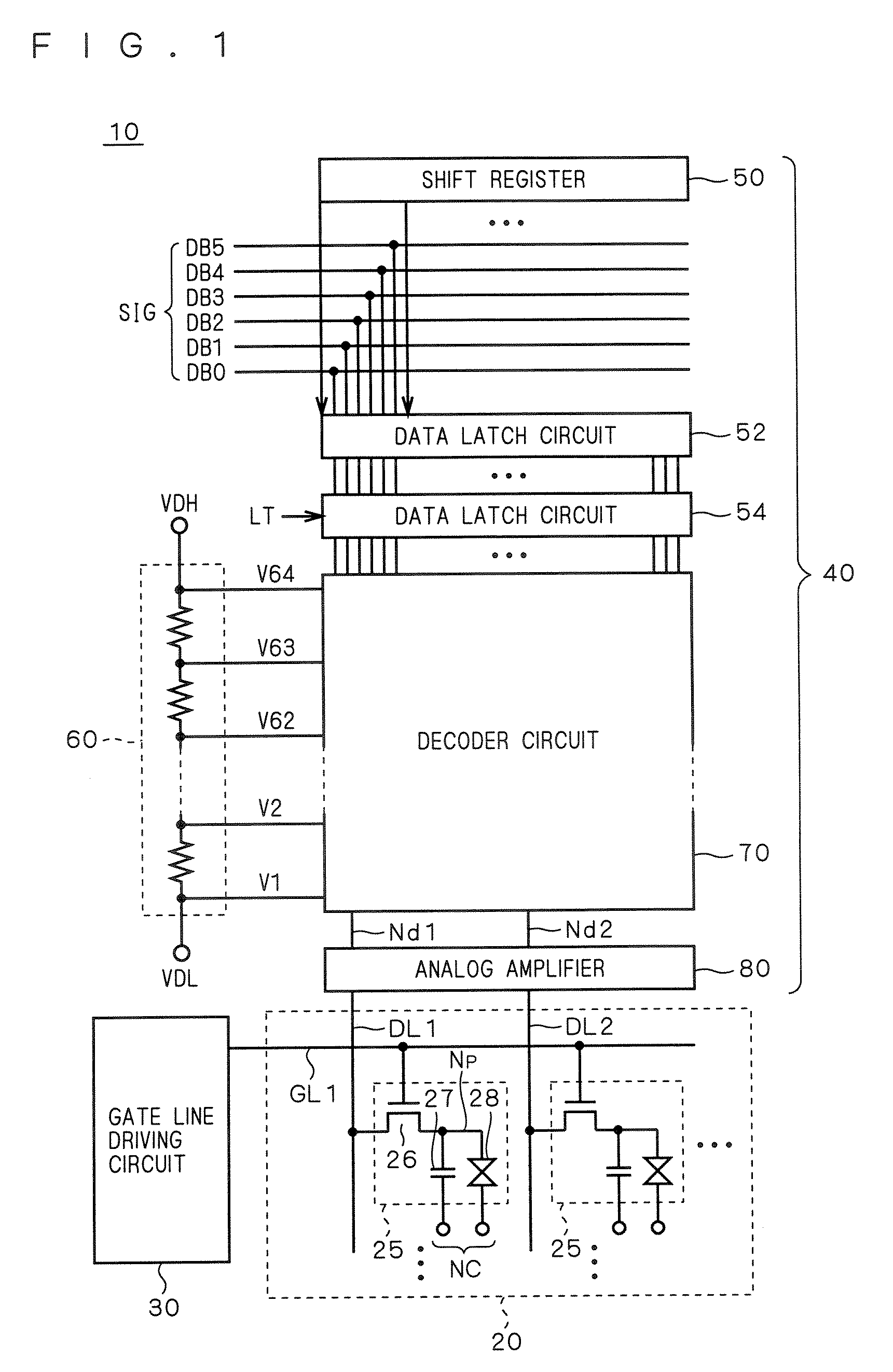
[0048]FIG. 1 is a schematic block diagram illustrating the configuration of a display apparatus according to a first preferred embodiment of the present invention, where the entire configuration of a liquid-crystal display apparatus 10 is illustrated as a typical example of a display apparatus.

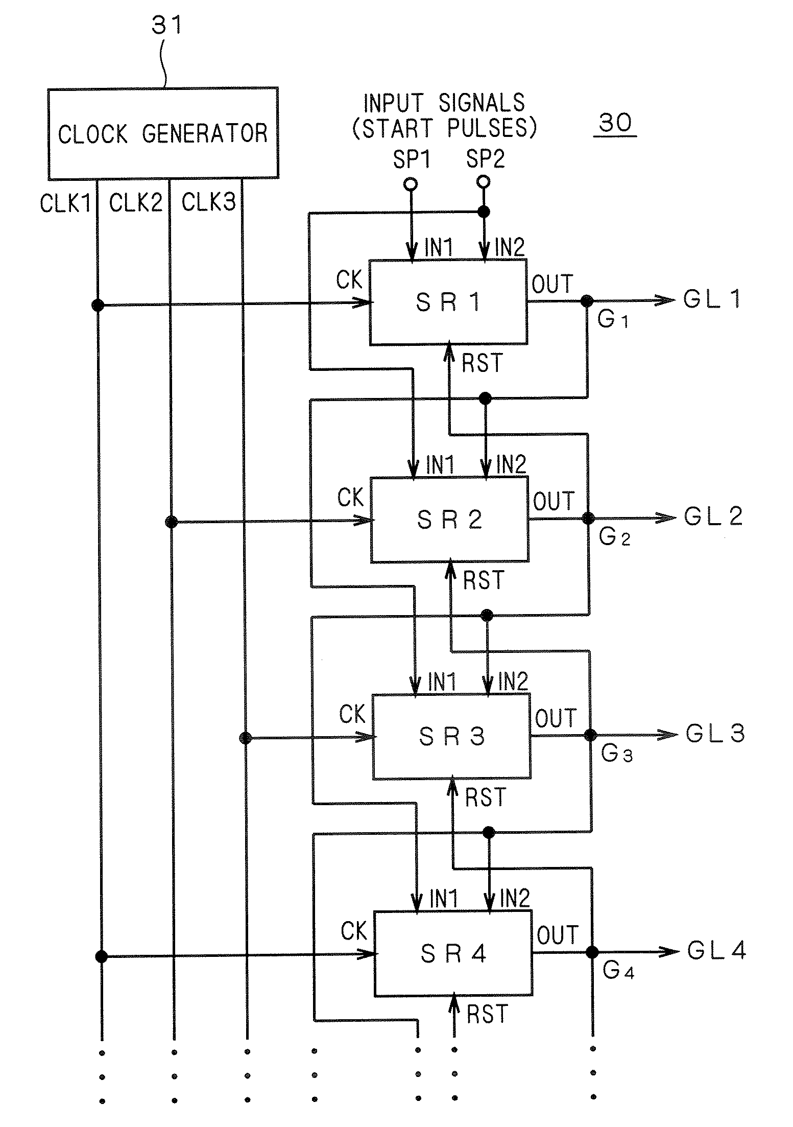
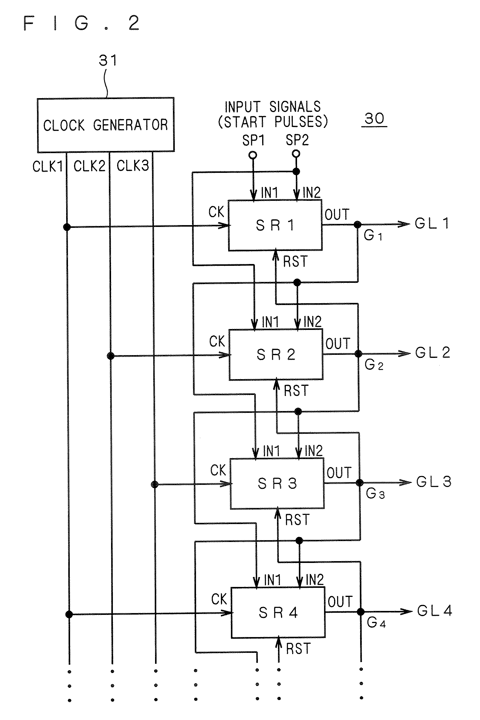
[0049]The liquid-crystal display apparatus 10 includes a liquid-crystal array 20, a gate line driving circuit (a scanning line driving circuit) 30, and a source driver 40. As will be clearly understood from the following description, the shift registers of the preferred embodiments of the present invention are provided in the gate line driving circuit 30.

[0050]The liquid-crystal array 20 includes a plurality of pixels 25 that are arranged in rows and columns. Gate lines GL1, GL2 . . . (collectively referred to as “gate lines GL”) are provided respectively for the rows of pixels (hereinafter referred to also as “pixel lines”), and data lines DL1, DL2 . . . (collectively referred to as “data lin...

second preferred embodiment

[0099]Field-effect transistors, including TFTs, are devices in which, when a voltage over the threshold voltage is applied to the gate electrode, a conductive channel is formed in the semiconductor substrate right under the gate electrode with a gate insulating film between them, and the conductive channel electrically connects the drain and source to achieve a conducting state. Accordingly, a field-effect transistor in the conducting state has a certain electrostatic capacitance (gate capacitance) between the gate and channel. That is, the field-effect transistor can function as a capacitive element in which the channel in the semiconductor substrate and the gate electrode serve as two electrodes and the gate insulating film serves as a dielectric layer. Such capacitive elements are called “MOS (Metal-Oxide Semiconductor) capacitive elements”.

[0100]FIG. 6 is a circuit diagram illustrating the configuration of a unit shift register circuit SR according to a second preferred embodime...

third preferred embodiment

[0108]In the unit shift register circuits SR of the first preferred embodiment, a charging circuit (the transistor Q8) and a boosting circuit (the capacitive element C2) are provided for the gate of the transistor Q3 (the node N3) that charges the node N1, whereby the node N3 is boosted to the level of 2×VDD−Vth. This causes the transistor Q3 to perform a non-saturated operation and so the node N1 can be rapidly charged (pre-charged).

[0109]In this preferred embodiment, this technique is applied also to the gate of the transistor Q8 that charges the node N3, where a charging circuit and a boosting circuit are provided also for the gate of the transistor Q8 so that the node N3 can be boosted to a still higher level than in the first preferred embodiment.

[0110]FIG. 7 is a circuit diagram illustrating the configuration of a unit shift register circuit according to a third preferred embodiment. In this preferred embodiment, too, the unit shift register circuit SR includes a charging circ...


PUM


Abstract

In a shift register circuit, a reduction of a driving capability caused by an increased operating rate is prevented. A shift register circuit includes a first transistor between an output terminal and a clock terminal, a second transistor between the output terminal and a first power-supply terminal, and a third transistor between the gate of the first transistor and a second power-supply terminal. The shift register circuit further includes a fourth transistor that charges the gate node of the third transistor on the basis of a signal inputted to a first input terminal, and a capacitive element that boosts the gate node of the third transistor that has been charged.

Description

BACKGROUND OF THE INVENTION[0001]1. Field of the Invention[0002]The present invention relates to a shift register circuit, and particularly to a shift register circuit that is formed of field-effect transistors of only the same conductivity type, for use in, e.g., a scanning line driving circuit of an image display apparatus.[0003]2. Description of the Background Art[0004]An image display apparatus (hereinafter “display apparatus”), such as a liquid-crystal display apparatus, has a display panel where a plurality of pixels are arranged in a matrix, and gate lines (scanning lines) are provided for individual rows of the pixels (pixel lines). The gate lines are sequentially selected and driven in cycles based on one horizontal period of the display signal, so as to update the displayed image. For the gate line driving circuit (scanning line driving circuit) for sequentially selecting and driving the pixel lines or gate lines, a shift register that performs one cycle of shift operation...

Claims


Application Information

Patent Timeline
IPC IPC(8): G11C19/00
CPCG11C19/28G11C19/184G09G3/20G11C19/00G09G3/36H03K19/00
Inventor TOBITA, YOUICHI
Owner TRIVALE TECH
Why Eureka
Try Eureka