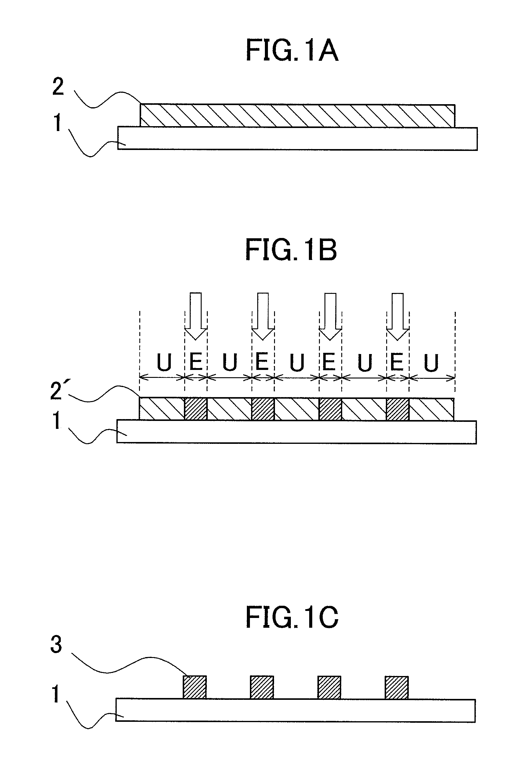
Resist composition for supercritical development
a composition and composition technology, applied in the direction of photomechanical treatment, instruments, photosensitive materials, etc., can solve the problems of forming patterns to collapse, pattern distortion, step distortion, swelling and pattern distortion, etc., to reduce pattern distortion and high aspect ratio
- Summary
- Abstract
- Description
- Claims
- Application Information
AI Technical Summary
Benefits of technology
Problems solved by technology
Method used
Image
Examples
example 1
Preparation of Resist Composition for Supercritical Development Process
[0129]A resist composition was obtained by dissolving 100 parts by mass of the resin represented by the following general formula (XI), 8.0 parts by mass of a compound represented by the following general formula (XII) as an acid generator, 1.60 parts by mass of tri-n-octylamine, and 0.64 parts by mass of salicylic acid in propylene glycol monomethyl ether acetate so that the concentration of the solid content was 5.0% by mass.
[0130]On a silicon wafer was coated the negative resist composition obtained as described above, using a spinner. After conducting a prebaking treatment at 100° C. for 90 seconds, the coated resist film having a film thickness of 150 nm was obtained through drying.
(Drawing)
[0131]Next, drawing of the pattern was carried out by irradiating an electron beam directly on the resulting coated resist film using an electron-beam drawing apparatus (manufactured by Hitachi Co., Ltd., trade name: HD-8...
example 2
Preparation of Resist Composition for Supercritical Development Process
[0135]A resist composition was obtained by dissolving 100 parts by mass of the resin represented by the following general formula (XIV), 6.0 parts by mass of a compound represented by the aforementioned general formula (XII) as an acid generator, 0.50 parts by mass of tri-n-octylamine, and 0.20 parts by mass of salicylic acid in propylene glycol monomethyl ether acetate so that the concentration of the solid content was 7.0% by mass.
[0136]On a silicon wafer was coated the resist composition obtained as described above, using a spinner. After conducting a prebaking treatment at 110° C. for 90 seconds, the coated film having a film thickness of 600 nm was obtained through drying.
(Drawing)
[0137]Next, drawing of the resist pattern was carried out by irradiating an electron beam directly on the resulting coated film using an electron-beam drawing apparatus (manufactured by Hitachi Co., Ltd., trade name: HL-800, accele...
PUM
| Property | Measurement | Unit |
|---|---|---|
| dispersity index | aaaaa | aaaaa |
| dispersity index | aaaaa | aaaaa |
| boiling point | aaaaa | aaaaa |
Abstract
Description
Claims
Application Information


