Method for manufacturing semiconductor device

a semiconductor device and manufacturing method technology, applied in the field of laser irradiation method, can solve the problems of increasing the drive voltage for writing, making normal writing impossible, and hard current flow, so as to improve the productivity of id chips or the like having the semiconductor device, improve the speed of writing data, and improve the productivity of semiconductor devices

Inactive Publication Date: 2007-08-23
SEMICON ENERGY LAB CO LTD
View PDF40 Cites 19 Cited by
  • Summary
  • Abstract
  • Description
  • Claims
  • Application Information

AI Technical Summary

Benefits of technology

[0021]The present invention makes it possible to irradiate a plurality of portions with laser beams by single irradiation, improve speed of writing data into a semiconductor device including a memory

Problems solved by technology

However, with respect to a memory circuit including a memory element provided with an organic compound between a pair of electrodes, in the case of writing data by electric action, there is a problem in that an organic compound layer having large film thickness makes it harder for current to flow, which increases drive voltage for writing, depending on the size of the memory circuit.
On the other hand, an organic compound layer having small film thickness makes it easier for current to be affected by dust or the shape of irregularities on the electrode layer surface, makes variations occur

Method used


Image

  • Method for manufacturing semiconductor device
  • Method for manufacturing semiconductor device
  • Method for manufacturing semiconductor device

Examples


embodiment modes

[0042]Embodiment modes of the present invention will be described with reference to the drawings. Note that the present invention can be implemented in many different forms, and it is easily understood by those skilled in the art that the modes and details can be variously modified without departing from the spirit and scope of the present invention. Therefore, the present invention is not construed as being limited to the description of Embodiment Modes. In all the drawings, the same reference numerals denote the same parts or the parts having similar functions, and the descriptions will not be repeated.

embodiment mode 1

[0043]In this embodiment mode, a method of writing data into a memory circuit area of a semiconductor device, in which the memory circuit area includes an organic compound, will be explained with reference to FIGS. 1 to 4B.

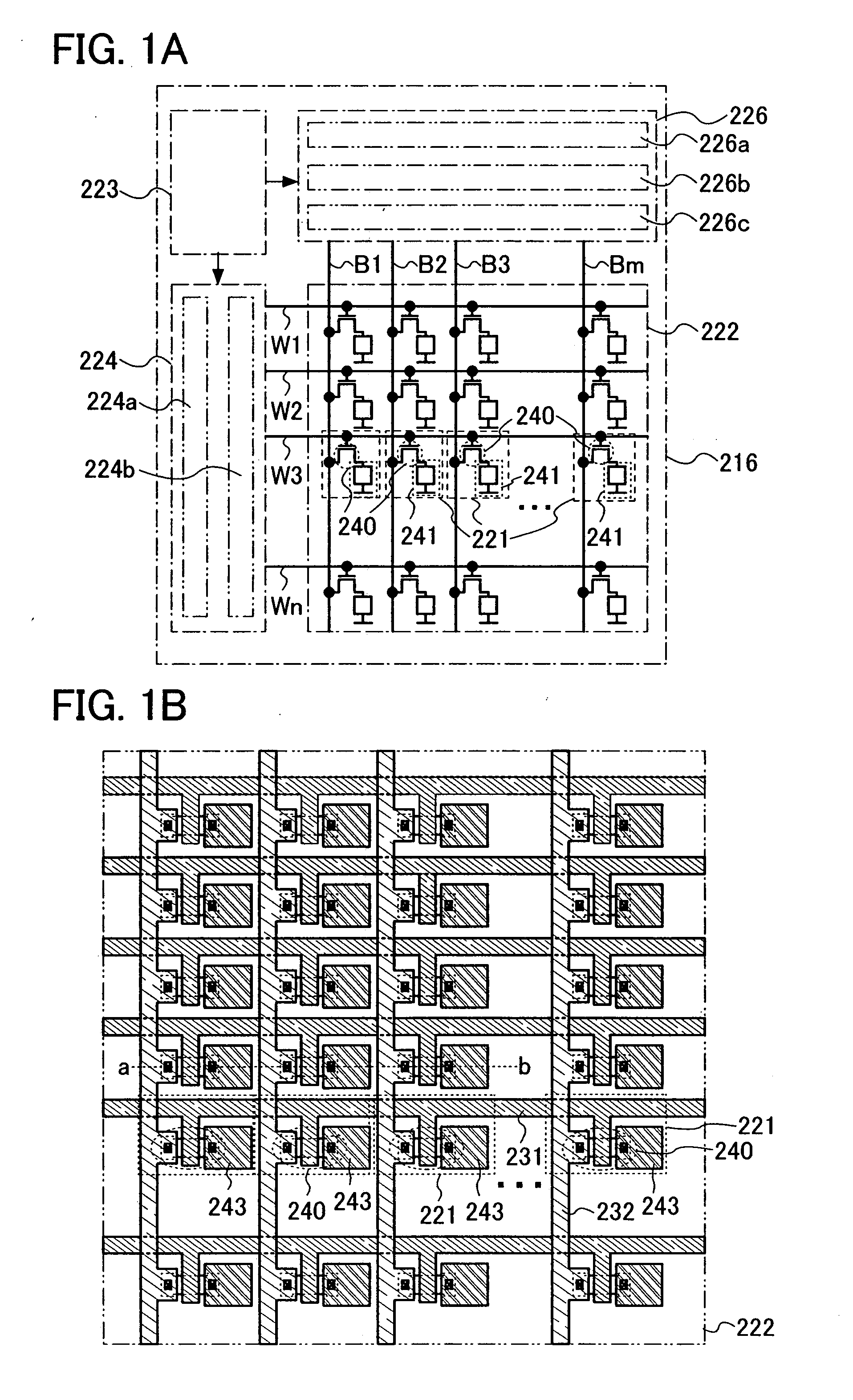
[0044]FIG. 1A is a schematic view of a semiconductor device having a memory circuit including a memory cell array 222 in which a plurality of memory cells 221 are arranged in matrix; a bit line driver circuit 226 including a column decoder 226a, a read circuit 226b, and a selector 226c; a word line driver circuit 224 including a row decoder 224a and a level shifter 224b; and an interface 223 having a writing circuit, which communicates with the external. Note that the structure shown here is only an example; accordingly, the memory circuit 216 may include another circuit such as a sense amplifier, an output circuit, or a buffer; alternatively, the wiring circuit may be provided in the bit line driver circuit.

[0045]The plurality of memory cells 221 each include at ...

embodiment mode 2

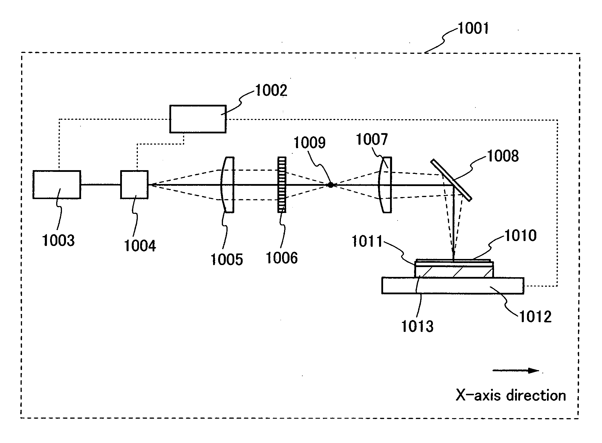
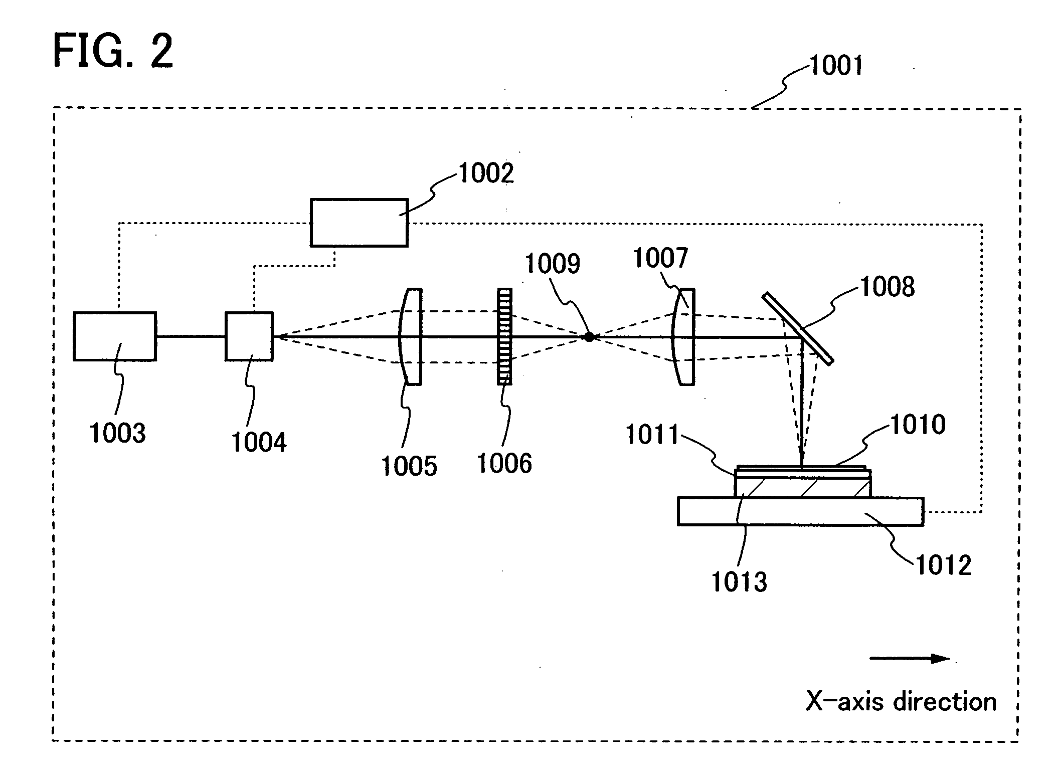
[0069]In this embodiment mode, a configuration of a laser irradiation apparatus having a different configuration from the laser irradiation apparatus for irradiating an organic compound layer with laser beams, which is shown in FIG. 2 will be described. A configuration of the apparatus and a method of laser irradiation using a reflective diffractive optical element as a diffractive optical element will be described with reference to FIG. 5.

[0070]FIG. 5 is a schematic diagram of a laser irradiation apparatus of this embodiment mode. A laser beam emitted from a laser oscillator 401 passes through a deflector. In this embodiment mode, an example of using an acousto-optic deflector (AOD) 402 as the deflector will be described. Note that the deflector used in the present invention is not limited to an AOD. For example, the direction of travel of a laser beam may be controlled by using a galvanometer mirror. An AOD is a device which deflects a laser beam by an acousto-optic effect in an o...


PUM

PropertyMeasurementUnit
Electrical resistanceaaaaaaaaaa
Electrical conductoraaaaaaaaaa
Reflectionaaaaaaaaaa

Abstract

To provide a method for manufacturing a semiconductor device using a method in which a desired position is rapidly subjected to laser irradiation while switching laser irradiation patterns. With respect to an organic memory element having a structure in which an organic compound layer is interposed between a pair of conductive layers, data is written to the organic memory element by laser irradiation using a laser irradiation apparatus. Further, a laser beam emitted from a laser oscillator is split by a diffractive optical element into a plurality of laser beams, thereby irradiating a plurality of portions on the organic compound layer with laser beams by single irradiation.

Description

BACKGROUND OF THE INVENTION[0001]1. Field of the Invention[0002]The present invention relates to a laser irradiation method for performing laser irradiation efficiently. Further, the present invention relates to a method for manufacturing a semiconductor device, which includes the process of laser irradiation.[0003]2. Description of the Related Art[0004]In recent years, individual recognition technology has attracted attention. For example, there is a technology to be applied to production and management, with which information such as a history of an object is clarified by giving an ID (identification code) to the individual object. Above all, the developments of semiconductor devices that can send and receive data without contact have been advanced. As such semiconductor devices, in particular, an RFID (abbreviation of Radio Frequency Identification) tag (also referred to as an ID tag, an IC tag, and IC chip, an RF (Radio Frequency) tag, a wireless tag, an electronic tag, or a wir...

Claims


Application Information

Patent Timeline
IPC IPC(8): H01L21/00
CPCB23K26/067B23K2201/40H01L51/0017G11C13/0014G11C13/04B82Y10/00B23K2101/40H10K71/231
Inventor TANAKA, KOICHIROOISHI, HIROTADA
Owner SEMICON ENERGY LAB CO LTD
Why Eureka
Try Eureka