Circuit device and method of manufacturing the same

a technology of circuit devices and connection parts, applied in the direction of final product manufacturing, sustainable manufacturing/processing, semiconductor/solid-state device details, etc., can solve the problems of solder connection parts that are weakened, solder sinks occur, etc., to reduce the occurrence of solder sinks and improve the connection reliability of solder connection parts.

Active Publication Date: 2007-09-06
SEMICON COMPONENTS IND LLC
View PDF45 Cites 39 Cited by
  • Summary
  • Abstract
  • Description
  • Claims
  • Application Information

AI Technical Summary

Benefits of technology

[0021] The present invention has been made in consideration for the foregoing problems. The present invention provides a circuit device which suppresses occ

Problems solved by technology

Thus, sink of the solder occurs.
Furthermore, strength of a so

Method used


Image

  • Circuit device and method of manufacturing the same
  • Circuit device and method of manufacturing the same
  • Circuit device and method of manufacturing the same

Examples


first embodiment

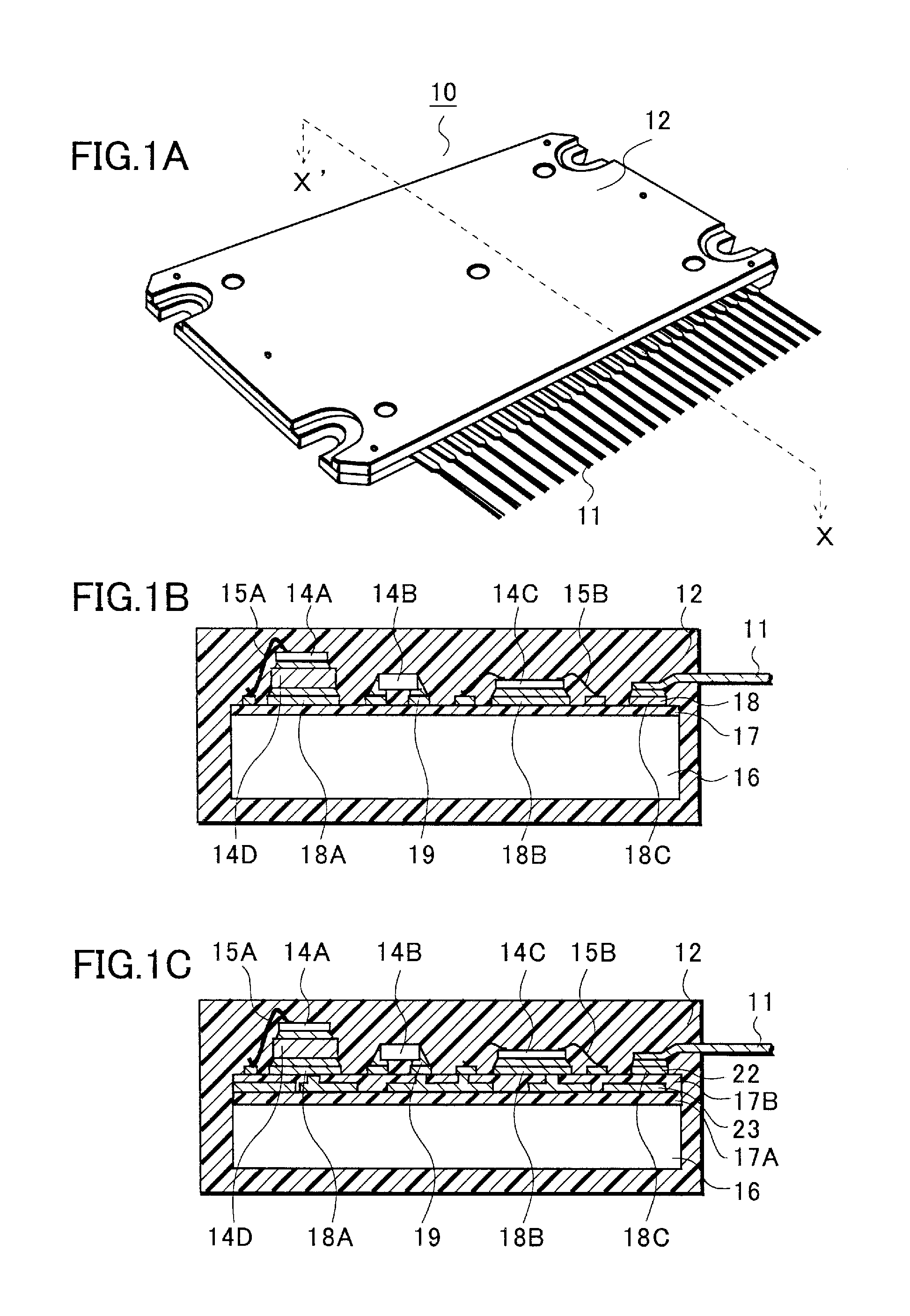
[0038] In this embodiment, with reference to FIGS. 1A to 1C, description will be given of a configuration of a hybrid integrated circuit device 10 that is a circuit device of the present invention. FIG. 1A is a perspective view of the hybrid integrated circuit device 10, FIG. 1B is a cross-sectional view thereof, and FIG. 1C is a cross-sectional view showing a heat sink 14D fixed to a pad 18A.

[0039] As shown in FIGS. 1A and 1B, in the hybrid integrated circuit device 10, a conductive pattern 18 is formed on a surface of a substrate 16, and a circuit element such as a transistor is fixed to the conductive pattern 18 with a solder 19 interposed therebetween. Moreover, at least the surface of the substrate 16 is covered with a sealing resin 12.

[0040] As the substrate 16, a metal substrate mainly made of aluminum, copper or the like, a substrate made of a resin material such as an epoxy resin, a substrate made of a flexible sheet, for example, a printed board, or the like is used. Mor...

second embodiment

[0053] In this embodiment, with reference to FIGS. 3 to 8, description will be given of a method of manufacturing the hybrid integrated circuit device 10 described above.

[0054] First Step: See FIGS. 3A and 3B

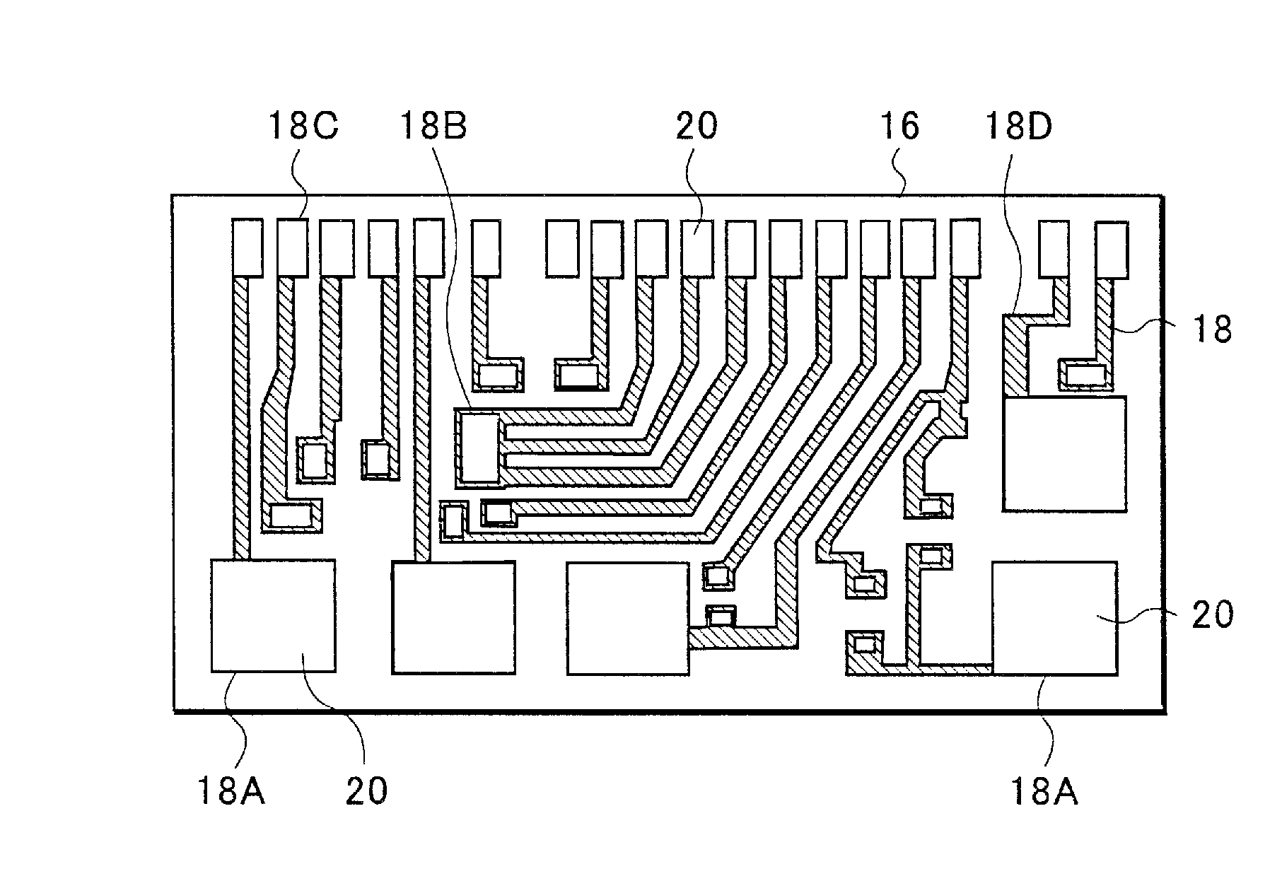
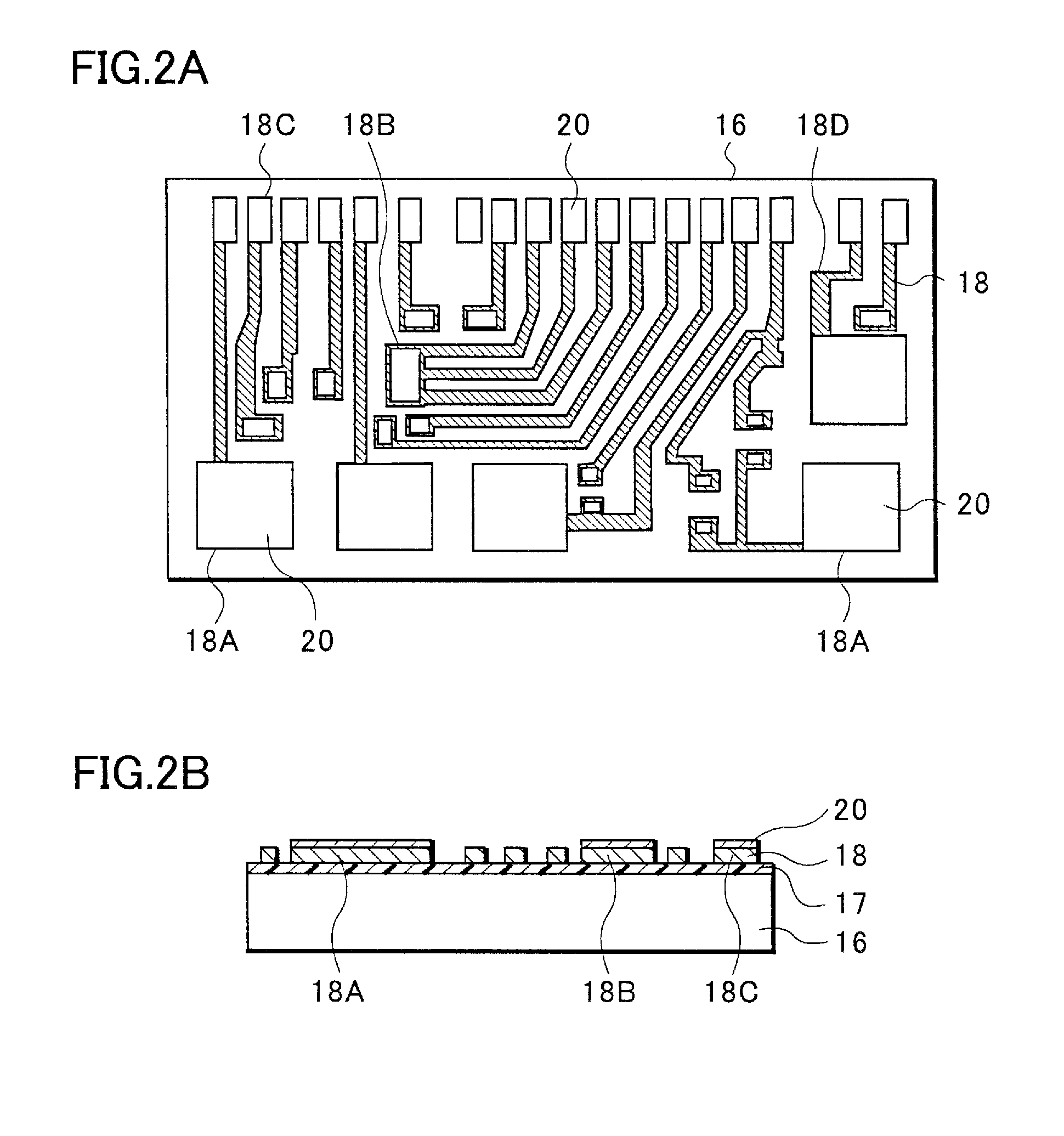
[0055] In this step, a conductive pattern 18 is formed on a surface of a substrate 16. FIG. 3A is a plan view of the substrate 16 in this step, and FIG. 3B is a cross-sectional view thereof.

[0056] As shown in FIGS. 3A and 3B, by patterning a conductive foil attached to the surface of the substrate 16, the conductive pattern 18 having a predetermined pattern shape is formed. Here, the conductive pattern 18 forms pads 18A to 18C. The pad 18A is a pad to which a heat sink is fixed in a subsequent step, and is formed to be relatively large. For example, the pad 18A is formed in a rectangular shape having a size of 9 mm×9 mm or more. The pad 18B is a pad to which a small signal transistor or a chip component is fixed, and is formed to be smaller than the pad 18A. For example, the p...

third embodiment

[0094] In this embodiment, description will be given of another method of manufacturing a hybrid integrated circuit device. Here, solder paste is collectively melted to fix circuit elements.

[0095] As shown in FIG. 9A, first, a substrate 16 on which a conductive pattern 18 is formed is prepared, and solder paste 21 is applied to desired pads. In this embodiment, the conductive pattern 18 forms pads 18A and 18B. The pad 18A is a pad to which a heat sink is fixed, and is formed to be as large as about 9 mm×9 mm or more, for example. The pad 18B is a pad to which a chip component such as a chip resistor or a small signal transistor is fixed, and is formed to be smaller than the pad 18A.

[0096] In this embodiment, a plated film 20 made of nickel is formed on a surface of the large pad 18A in which sink is likely to occur. Therefore, even if the solder paste 21 is melted, a Cu / Sn alloy layer having poor soldering properties is not formed. In this embodiment, a Ni / Sn alloy layer having so...


PUM

PropertyMeasurementUnit
Electrical conductoraaaaaaaaaa
Wettabilityaaaaaaaaaa

Abstract

In a hybrid integrated circuit device that is a circuit device of the present invention, a conductive pattern including pads is formed on a surface of a substrate. A first pad is formed to be relatively large since a heat sink is mounted thereon. A second pad is a small pad to which a chip component or a small signal transistor is fixed. In the present invention, a plated film made of nickel is formed on a surface of the first pad. Therefore, the first pad and a solder never come into contact with each other. Thus, a Cu/Sn alloy layer having poor soldering properties is not generated but a Ni/Sn alloy layer having excellent soldering properties is generated. Consequently, occurrence of sink in the melted solder is suppressed.

Description

CROSS-REFERENCE TO RELATED APPLICATIONS [0001] Priority is claimed to Japanese Patent Application Numbers JP2005-023328, filed on Jan. 31, 2005, and JP2005-346916, filed on Nov. 30, 2005, the disclosures of which are incorporated herein by reference in its entireties. BACKGROUND OF THE INVENTION [0002] 1. Field of the Invention [0003] The present invention relates to a circuit device and a method of manufacturing the same, and more particularly relates to a circuit device in which large circuit elements are connected with solder and a method of manufacturing the same. [0004] 2. Description of the Related Art [0005] With reference to FIGS. 10A to 11B, a method of manufacturing a conventional circuit device will be explained. Here, description will be given of a method of manufacturing a hybrid integrated circuit device in which a conductive pattern 108 and circuit elements are formed on a surface of a substrate 106. This technology is described for instance in Japanese Patent Applica...

Claims


Application Information

Patent Timeline
IPC IPC(8): H05K1/16H05K7/00
CPCH05K3/243Y10T29/49155H05K3/284H05K3/341H05K3/3463H05K2201/0391H05K2201/10969H01L2224/45124H05K3/244Y10T29/4913H01L2924/30107H01L2224/83H01L2924/01327H01L2924/01322H01L2924/19105H01L2224/73265H01L2224/48472H01L2224/48227H01L2224/48091H01L24/83H01L2924/00014H01L2924/00H01L2224/2612H01L2924/14H01L2924/15787Y02P70/50H01L25/04H01L25/18
Inventor TAKAKUSAKI, SADAMICHISAKAMOTO, NORIAKINEZU, MOTOICHIIGARASHI, YUSUKE
Owner SEMICON COMPONENTS IND LLC
Why Eureka
Try Eureka