

Single-photon generating device, single-photon detecting device, and optical quantum gate
- Summary
- Abstract
- Description
- Claims
- Application Information
AI Technical Summary
Benefits of technology
Problems solved by technology
Method used
Image

Examples
first embodiment
[0044]Hereinafter, the single-photon generating device according to a first embodiment of the present invention will be described referring to FIGS. 1 to 7.
[0045]The single-photon generating device according to the present embodiment is an optically pumped (PL) single-photon generating device using light emission from a quantum dot in a semiconductor substrate.
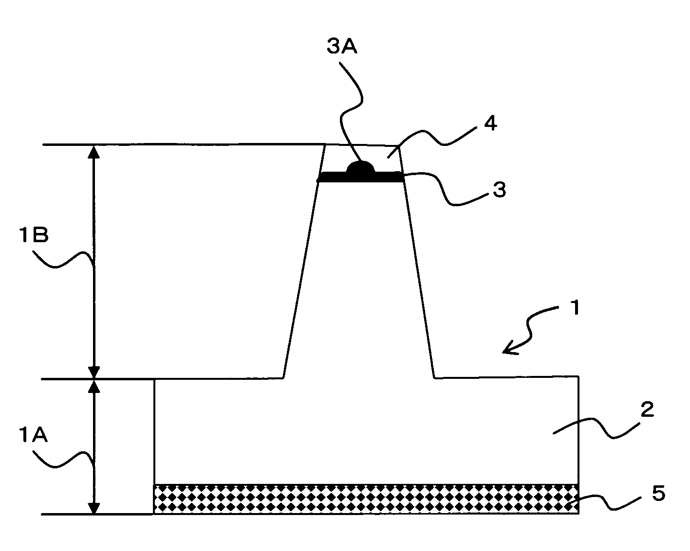
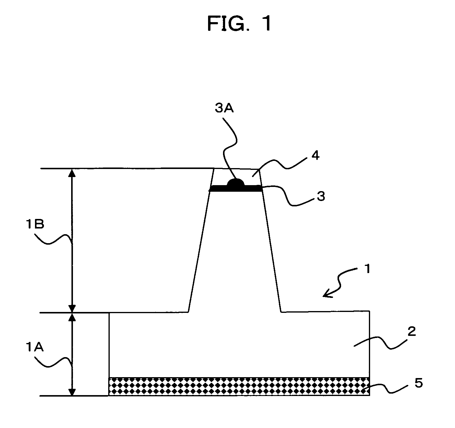
[0046]According to the present embodiment, a semiconductor substrate (solid substrate) 1 including an epitaxial growth layer constituted of a semiconductor material, for example, the InP related semiconductor material is used, as shown in FIG. 1. The above semiconductor substrate 1 is constituted of an i-InP substrate (including an i-InP layer) 2 on which an InAs layer 3, as quantum dot layer, and an i-InP layer 4 are laminated (stacked), as exemplarily shown in FIG. 1.
[0047]Also, according to the present embodiment, as shown in FIG. 1, the semiconductor substrate 1 includes a base portion 1A, a pillar portion 1B being formed ...
second embodiment
[0110]Next, a single-photon generating device according to a second embodiment of the present invention will be described referring to FIGS. 8(a)-8(d).
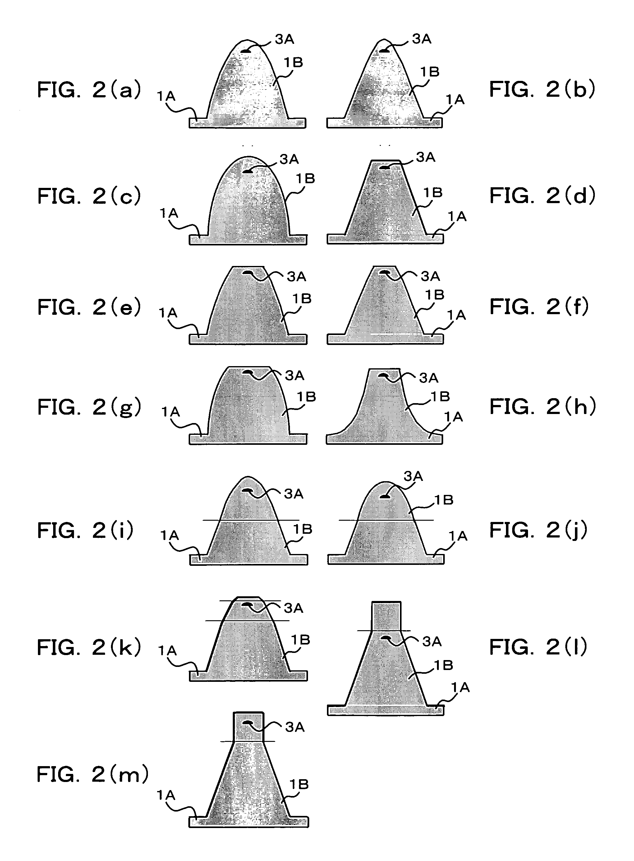
[0111]The manufacturing method of the single-photon generating device according to the present embodiment is different from the manufacturing method of the single-photon generating device according to the first embodiment. Namely, according to the present embodiment, by combining dry etching with wet etching having different anisotropy in the processing process of the surface side, the shape of the pillar portion 1B, in particular, an angle of the side face (slope face) can be adjusted, while aiming to reduce etching damage also.
[0112]According to the present embodiment, in the process for forming the pillar portion 1B, one or more wet etching processes having different etching conditions are used in combination with one or more dry etching processes having different etching conditions.
[0113]Hereafter, the manufacturing method of the ...
third embodiment
[0129]Next, a single-photon generating device according to a third embodiment of the present invention will be described referring to FIGS. 10 and 11(a)-11(o).
[0130]As compared to the aforementioned first embodiment, the single-photon generating device according to the present embodiment differs in the point that the device of interest is a single-photon generating device of current injection type (for example, current-injection EL device). Namely, the single-photon generating device according to the present embodiment is a current-injection single-photon generating device using the light emitted from the quantum dot (quantum dot capable of emitting a single photon) in the semiconductor substrate.
[0131]According to the present embodiment, as shown in FIG. 10, a semiconductor substrate (solid substrate) 10 including an epitaxial growth layer formed of a semiconductor material of, for example, the GaAs system is used. As exemplarily shown in FIG. 10, the semiconductor 10 has a p-i-n s...
PUM
 Abstract
Description
Claims
Application Information