
Semiconductor device and semiconductor device manufacturing method

a semiconductor device and manufacturing method technology, applied in the direction of semiconductor devices, basic electric elements, electrical appliances, etc., can solve the problems of reducing the thickness of the gate insulating film, reducing the efficiency of the gate electrode, so as to improve the productivity reduce the threshold voltage of the p channel misfet, and high dielectric constant film

Inactive Publication Date: 2007-09-13
RENESAS TECH CORP
View PDF3 Cites 80 Cited by
  • Summary
  • Abstract
  • Description
  • Claims
  • Application Information

AI Technical Summary

Benefits of technology

[0006]To get around this problem, by the use of a material with a dielectric constant higher than that of the silicon oxide film, a high dielectric-constant film having an increased physical film thickness even with the same capacity has been used. Since the physical film thickness can be increased even with the same capacity when using such a high dielectric-constant film, it is possible to reduce the leakage current.
[0014]An object of the present invention is to provide a technology capable of achieving an improvement in productivity of a p channel MISFET in which a high dielectric-constant film is used for the gate insulating film and a conductive film containing metal is used for the gate electrode. Also, another object of the present invention to provide a technology capable of decreasing a threshold voltage of the p channel MISFET even if a work function value of the conductive film containing metal at the time of contacting a silicon oxide film is away from a value near a valence band of silicon.
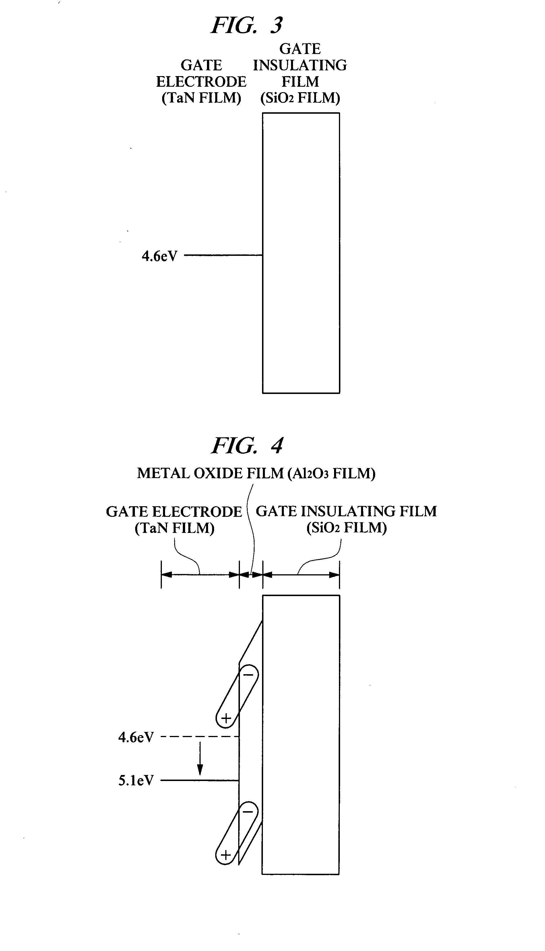
[0020]In a p channel MISFET using a high dielectric-constant film for the gate insulating film and a conductive film containing metal for the gate electrode, a high-quality conductive film formed through a semiconductor process can be used for the gate electrode. Therefore, productivity can be increased. Also, an insulating metal oxide film is formed between the gate insulating film and the gate electrode, thereby forming a dipole between the gate electrode and the metal oxide film. Therefore, the threshold voltage of the p channel MISFET can be decreased even if a work function value of the conductive film containing metal at the time of contacting a silicon oxide film is away from a value near a valence band of silicon.

Problems solved by technology

However, in recent years, with the development in microfabrication of MISFETs, the thickness of the gate insulating film has been more and more reduced, and depletion of the gate electrode when a polysilicon film is used for the gate electrode has become nonnegligible.

Method used


Image

  • Semiconductor device and semiconductor device manufacturing method
  • Semiconductor device and semiconductor device manufacturing method
  • Semiconductor device and semiconductor device manufacturing method

Examples


Embodiment Construction

[0039]In the embodiments described below, the invention will be described in a plurality of sections or embodiments when required as a matter of convenience. However, these sections or embodiments are not irrelevant to each other unless otherwise stated, and the one relates to the entire or a part of the other as a modification example, details, or a supplementary explanation thereof.

[0040]Also, in the embodiments described below, when referring to the number of elements (including number of pieces, values, amount, range, and the like), the number of the elements is not limited to a specific number unless otherwise stated or except the case where the number is apparently limited to a specific number in principle. The number larger or smaller than the specified number is also applicable.

[0041]Further, in the embodiments described below, it goes without saying that the components (including element steps) are not always indispensable unless otherwise stated or except the case where th...


PUM


Abstract

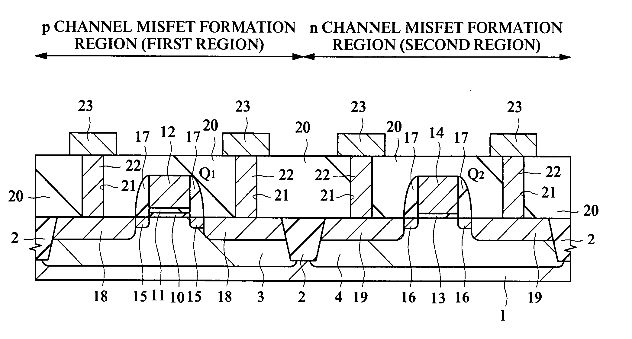
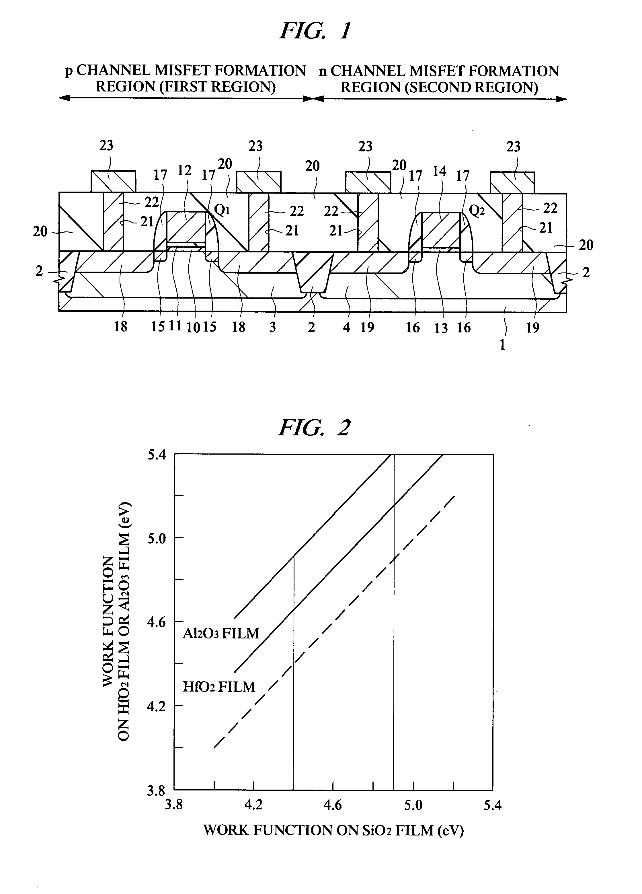
Provided is a technology capable of improving the productivity of a p channel MISFET using a high dielectric-constant film as a gate insulating film and a conductive film containing metal as a gate electrode. In this technology, a threshold voltage of the p channel MISFET can be decreased even if a work function value of the conductive film containing metal at the time of contacting a silicon oxide film is away from a value near a valence band of silicon. A p channel MISFET formed on a semiconductor substrate has a gate insulating film formed of a hafnium oxide film, a metal oxide film formed of an aluminum oxide film on this gate insulating film, and a gate electrode formed of a tantalum nitride film on this metal oxide film. The metal oxide film has a function to shift a work function value of the gate electrode.

Description

CROSS-REFERENCE TO RELATED APPLICATION[0001]The present application claims priority from Japanese Patent Application No. JP 2006-65674 filed on Mar. 10, 2006, the content of which is hereby incorporated by reference into this application.TECHNICAL FIELD OF THE INVENTION[0002]The present invention relates to semiconductor devices and semiconductor device manufacturing technologies. In particular, it relates to a technology effectively applied to a MISFET (Metal Insulator Semiconductor Field Effect Transistor) using a conductive film containing metal for a gate electrode.BACKGROUND OF THE INVENTION[0003]Japanese Patent Application Laid-Open Publication No. 2005-294422 (Patent Document 1) discloses a technology capable of, when metal is used for the gate electrode material of a MISFET, preventing reaction or exfoliation between metal and a gate insulating film and controlling a threshold voltage of the MISFET.[0004]Specifically, the MISFET includes a gate insulating film formed on a se...

Claims


Application Information

Patent Timeline
Patent Type & Authority Applications(United States)
IPC IPC(8): H01L29/76
CPCH01L21/823842H01L29/517H01L21/823857
Inventor NABATAME, TOSHIHIDEKADOSHIMA, MASARU
Owner RENESAS TECH CORP
Learn More