Surface-discharge-type plasma display panel

a plasma display panel and surface-discharge technology, which is applied in the direction of gas discharge filling, gas discharge vessel/container, gas discharge tube, etc., can solve the problems of serious problems such as the occurrence of luminance residual images, the degradation of image display quality, and the increase of the time of discharge delay, so as to improve the light-emitting efficiency of the panel, the effect of improving the discharge delay characteristics

Inactive Publication Date: 2007-09-13
PANASONIC CORP
View PDF7 Cites 15 Cited by
  • Summary
  • Abstract
  • Description
  • Claims
  • Application Information

AI Technical Summary

Benefits of technology

[0026]According to this aspect, the discharge gas filling the discharge space is a high-xenon gas including 10% or more xenon by volume, and also the dielectric layer is formed of a low-relatively-dielectric-constant dielectric material having a relative dielectric constant of 9 or less, thereby making it possible to achieve a significant high light emitting efficiency as compared with that in conventional PDPs. In addition, the protective layer covering the dielectric layer includes a magnesium oxide crystal, thus making it possible to eliminate the occurrence of discharge delay which results from then increase in xenon in the discharge gas and the reduction in the relative dielectric constant of the dielectric material, and also to further achieve an improvement in discharge delay characteristics as compared with conventional PDPs.
[0027]In the PDP according to the aspect, the dielectric material used for forming the dielectric layer is preferably a leadless glass material having

Problems solved by technology

This increase in the discharge intensity causes a luminance residual image, resulting in degradation in the display quality of the images.
In particular, the occurrence of a luminance residual image is a serious problem for a PDP which repeats discharges many times within a frame display period in order to achieve the gradation display based on the above-described subfield method.
How

Method used


Image

  • Surface-discharge-type plasma display panel
  • Surface-discharge-type plasma display panel
  • Surface-discharge-type plasma display panel

Examples


Embodiment Construction

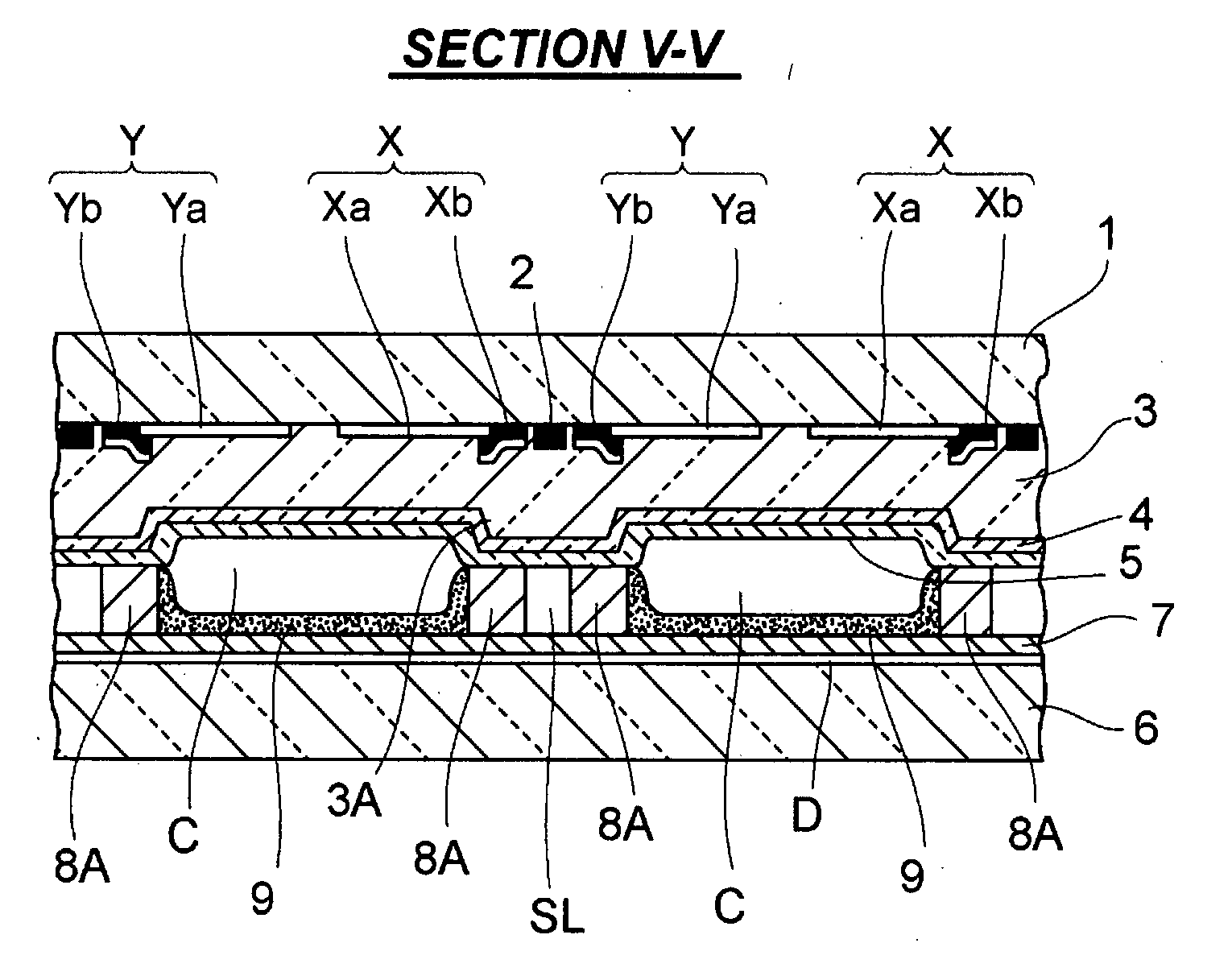
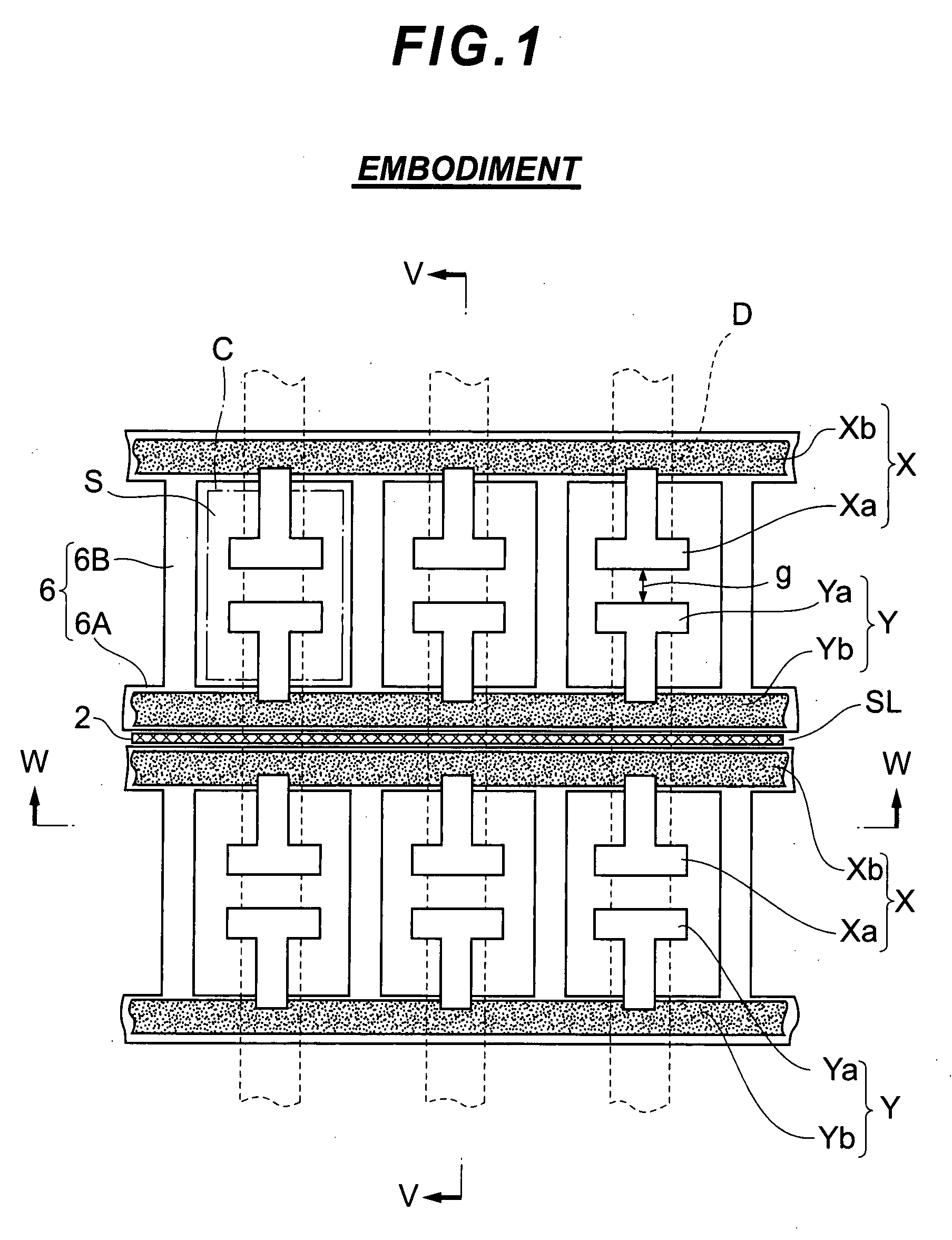
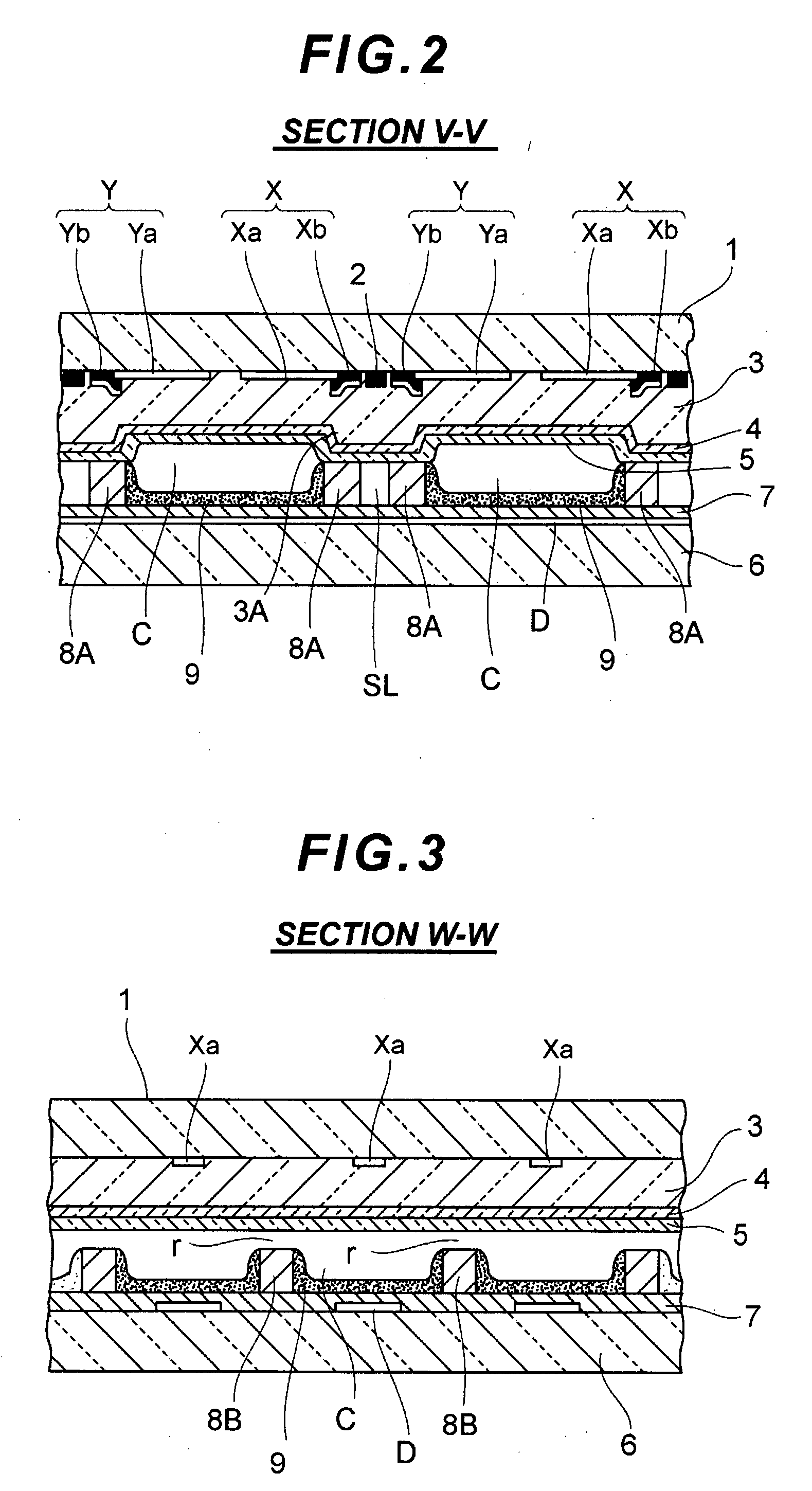
[0051]FIGS. 1 to 3 illustrate an example of a preferred embodiment of the PDP according to the present invention. FIG. 1 is a schematic front view of the PDP in the embodiment example. FIG. 2 is a sectional view taken along the V-V line in FIG. 1. FIG. 3 is a sectional view taken along the W-W line in FIG. 1.

[0052]The PDP in FIGS. 1 to 3 has a plurality of row electrode pairs (X, Y) arranged in parallel on the rear-facing face of a front glass substrate 1 serving as the display surface so as to extend in the row direction of the front glass substrate 1 (the right-left direction in FIG. 1).

[0053]A row electrode X is composed of T-shaped transparent electrodes Xa formed of a transparent conductive film made of ITO or the like, and a bus electrode Xb formed of a metal film extending in the row direction of the front glass substrate 1 and connected to the narrow proximal ends of the transparent electrodes Xa.

[0054]Likewise, a row electrode Y is composed of T-shaped transparent electrode...


PUM


Abstract

For improvement in the performance of a PDP, a dielectric layer, deposited on the inner face of the front glass substrate of the PDP and covering row electrode pairs, is formed of a dielectric material having a relative dielectric constant of 9 or less, and a protective layer overlying the dielectric layer includes a magnesium oxide crystal causing a cathode-luminescence emission having a peak within a wavelength range of 200 nm to 300 nm upon excitation by electron beams, and discharge gas filling the discharge space includes 10% or more xenon by volume.

Description

BACKGROUND OF THE INVENTION[0001]1. Field of the Invention[0002]This invention relates to the structure of surface-discharge-type plasma display panels.[0003]The present application claims priority from Japanese Applications No. 2006-066129 and No. 2006-066130, the disclosure of which is incorporated herein by reference.[0004]2. Description of the Related Art[0005]A surface-discharge-type alternating-current plasma display panel (hereinafter referred to as “PDP”) includes two opposing glass substrates placed on either side of a discharge space. On one of the two glass substrates a plurality of row electrode pairs, which extend in the row direction, are regularly arranged in the column direction and covered by a dielectric layer. On the dielectric layer a magnesium oxide film having the function of protecting the dielectric layer and the function of emitting secondary electrons into the discharge space is formed by a vapor deposition technique. On the other glass substrate, a plurali...

Claims


Application Information

Patent Timeline
IPC IPC(8): H01J17/49H01J17/20
CPCH01J11/12H01J11/40H01J11/38H01J11/50
Inventor MIYATA, TAKASHIKAMO, YOSHIHIKOTABUCHI, HIROTOSHITOKAIRIN, HIROAKI
Owner PANASONIC CORP
Why Eureka
Try Eureka