Display Device and Method for Driving the Same

a technology of display device and drive device, which is applied in the direction of power management, high-level techniques, instruments, etc., can solve the problems of cost reduction by curtailing processes, and achieve the effects of reducing costs, curtailing processes, and small siz

Active Publication Date: 2007-09-13
SEMICON ENERGY LAB CO LTD
View PDF53 Cites 38 Cited by
  • Summary
  • Abstract
  • Description
  • Claims
  • Application Information

AI Technical Summary

Benefits of technology

[0012] The display device in which TFTs are formed on a substrate and a pixel part and peripheral circuits are built in one piece is applied to mobile devices in significant growth, taking advantage of its small size and lightweight. At the same time,

Problems solved by technology

At the same time, TFTs are formed through many processes such as film deposition, device fabrication by repeating etching, and injectio

Method used


Image

  • Display Device and Method for Driving the Same
  • Display Device and Method for Driving the Same
  • Display Device and Method for Driving the Same

Examples


embodiment 1

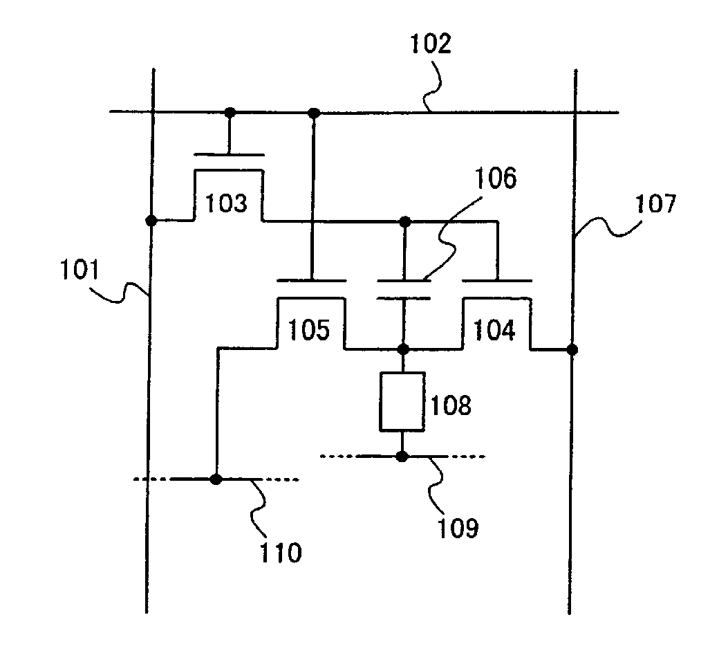
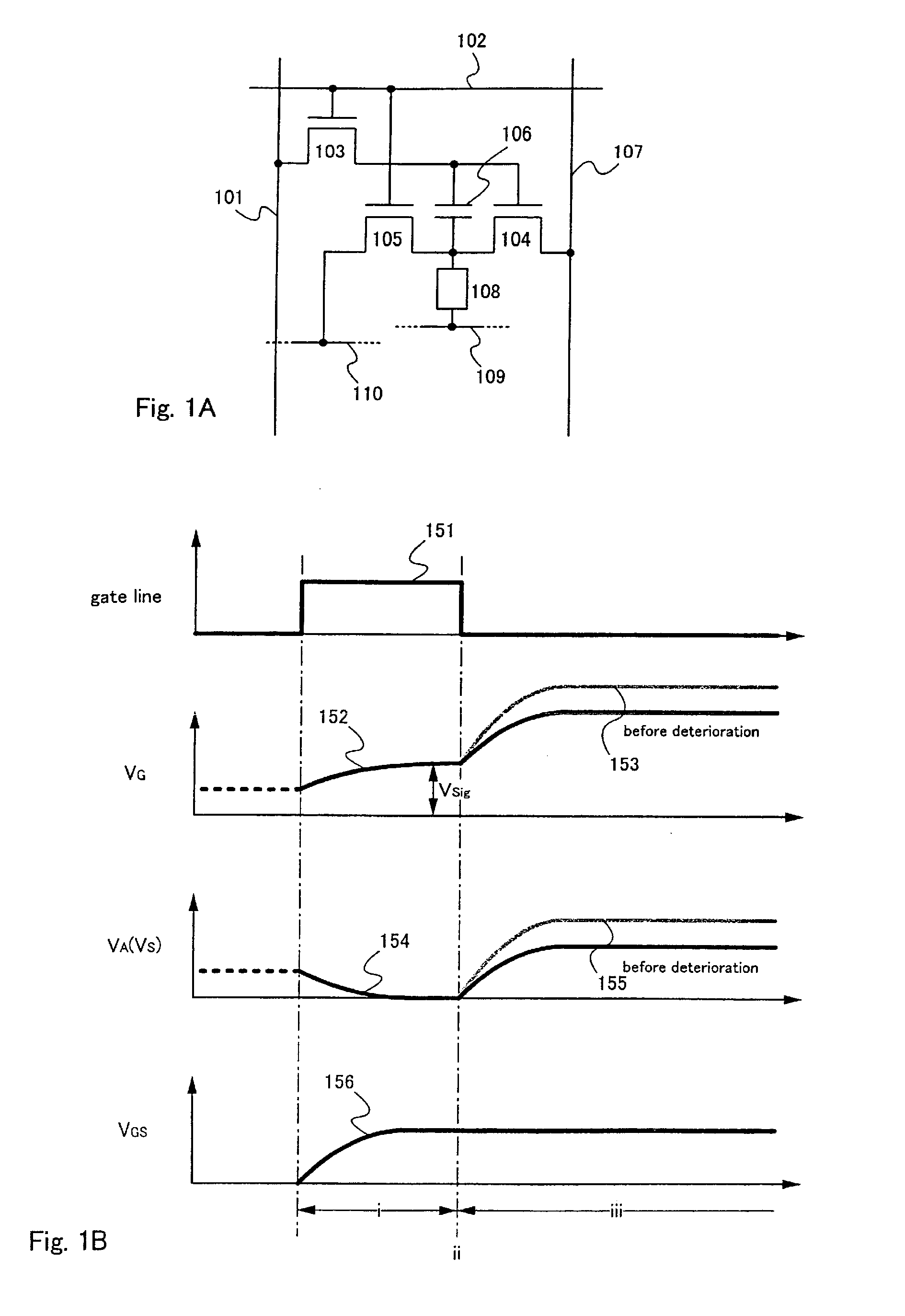
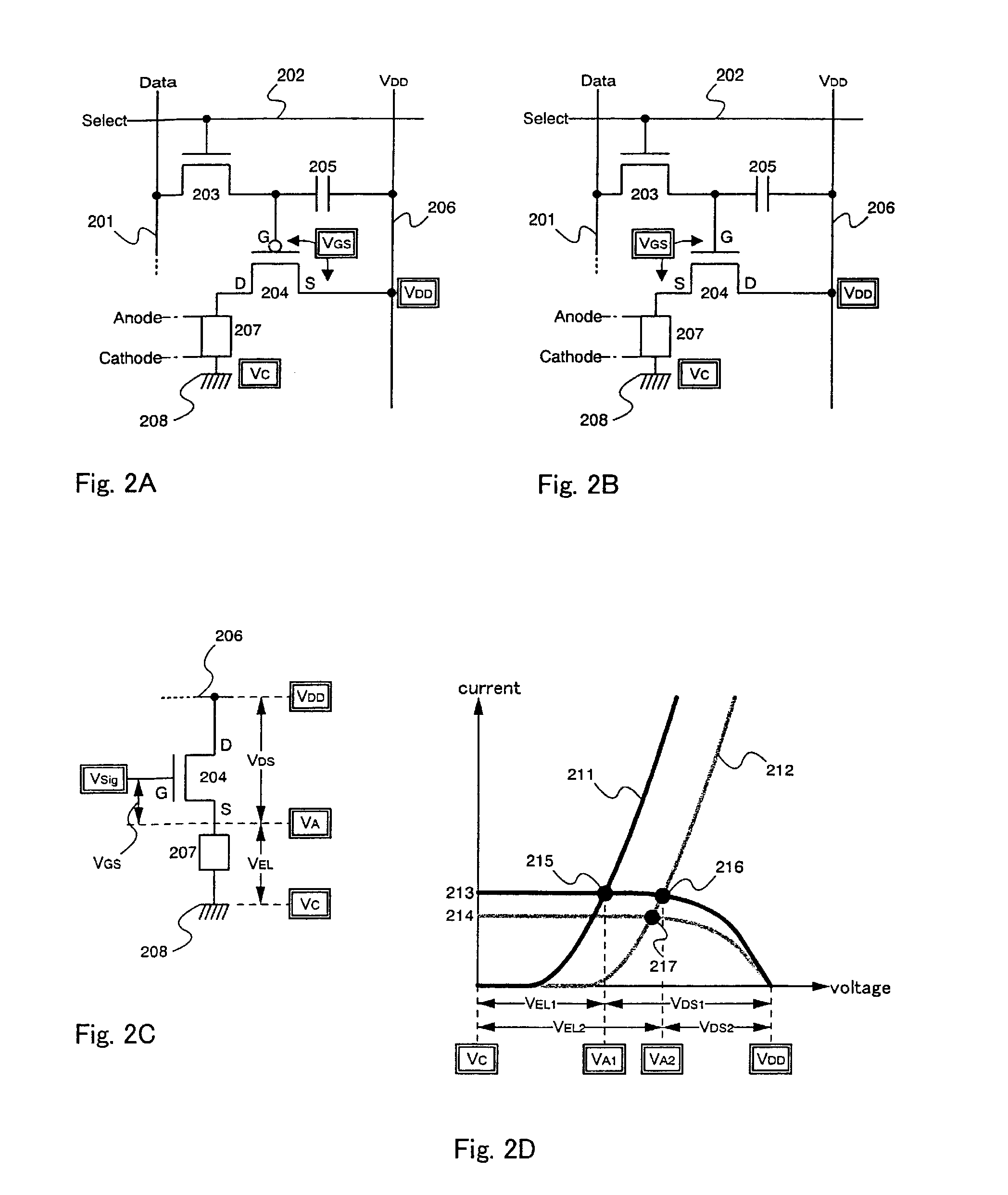
[0203]FIG. 1A depicts an embodiment of the invention. The pixel of the invention has a source signal line 101, a gate signal line 102, first, second and third TFTs 103 to 105, a capacitance element 106, a current supply line 107, an EL element 108, and power source lines 109 and 110. The gate electrode of the TFT 103 is connected to the gate signal line 102, the first electrode of the TFT 103 is connected to the source signal line 101, and the second electrode of the TFT 103 is connected to the gate electrode of the TFT 104. The first electrode of the TFT 104 is connected to the current supply line 107, and the second electrode of the TFT 104 is connected to the first electrode of the TFT 105 and the first electrode of the EL element. The gate electrode of the TFT 105 is connected to the gate signal line 102, and the second electrode of the TFT 105 is connected to the power source line 110. The second electrode of the EL element 108 is connected to the power source line 109. The cap...

embodiment 2

[0217] According to the configuration shown in FIG. 1A, for the lines routed to the pixel part, five lines were needed: the source signal line, the gate signal line, the current supply line (VDD), the power source line (VC), and the power source line (VSS). In this embodiment, the configuration will be described in which lines for wiring are shared, whereby allowing the number of lines for wiring per pixel to be reduced and high numerical aperture to be obtained.

[0218]FIG. 9 depicts the configuration of the embodiment. The point different from the embodiment 1 is only the point in that the second electrode of a TFT 906 is connected to the power source line (VSS) but it is connected to the gate signal line in a pixel of the next row in the embodiment. Suppose the pixel expressed by a dotted frame 900 is in the ith row, the second electrode of the TFT 906 is connected to the gate signal line in the i+1st row.

[0219] As the pulse condition of selecting the gate signal line, it is acce...

embodiment 3

[0223] It is called the analogue gray scale system that the gate-source voltage of a driving TFT is controlled, and the current value carried through an EL element is controlled by analogue quantity for display. In the meantime, the digital gray scale system is proposed in which an EL element is driven only by two states, a hundred or zero percent luminance. In this system, only two levels of gray scale, black and white, can be displayed, but it has a merit of hardly being subject to variations in the TFT characteristics. To intend to have the multiple gray scale by the digital gray scale system, a driving method of combining with the time gray scale system is used. The time gray scale system is the method of expressing the gray scale by the length of time that the element emits light for a long time or short time.

[0224] When the digital gray scale system is combined with the time gray scale system, one frame period is split into a plurality of subframe periods as shown in FIG. 10A...


PUM


Abstract

A semiconductor device having a configuration hardly generating variations in the current value due to a deteriorated EL element is to be provided. A capacitance element is disposed between the gate and the source of a driving TFT, video signals are inputted to the gate electrode, and then it is in the floating state. At this time, when the gate-source voltage of the driving TFT exceeds the threshold, the driving TFT is turned on. Suppose an EL element is deteriorated and the anode potential rises, that is, the source potential of the driving TFT rises, the potential of the gate electrode of the driving TFT, being in the floating state by coupling of the capacitance element, is to rise by the same amount. Accordingly, even when the anode potential rises due to the deteriorated EL element, the rise is added to the gate electrode potential as it is, and the gate-source voltage of the driving TFT is allowed to be constant.

Description

BACKGROUND OF THE INVENTION [0001] The present invention relates to the configuration of a semiconductor device having a transistor. The invention also relates to the configuration of an active matrix display device including a semiconductor device having a thin film transistor (hereafter, it is denoted by TFT) fabricated on an insulator such as glass and plastics. In addition, the invention relates to an electronic device using such the display device. [0002] In recent years, the development of display devices using light emitting elements including electroluminescent (EL) elements has been conducted actively. The light emitting element has high visibility because it emits light for itself. It does not need a back light that is needed in liquid crystal display devices (LCD), and thus it is suitable for forming to have a low profile and has nearly no limits to the field of view. [0003] Here, the EL element is an element having a light emitting layer that can obtain luminescence gene...

Claims


Application Information

Patent Timeline
IPC IPC(8): G09G3/00G09G3/20G09G3/30G09G3/32H01L27/32H04M1/73H05B44/00
CPCG09G3/2022H01L27/1255G09G3/3266G09G3/3291G09G2300/0426G09G2300/0842G09G2310/0251G09G2310/0256G09G2310/027G09G2310/061G09G2320/043G09G2330/08G09G2330/10H01L27/3244H04W52/027G09G3/3233Y02D30/70H10K59/12G09G3/30
Inventor KIMURA, HAJIME
Owner SEMICON ENERGY LAB CO LTD
Why Eureka
Try Eureka