

Method for determining an edge profile of a volume of a photoresist after a development process
a technology of photoresist and volume, applied in the field of method for determining can solve the problems of limited practical application of conventional simulation methods in order to predict the edge profile of a volume of a photoresist after a development process, and the general requirements of high computing time of conventional simulation methods
- Summary
- Abstract
- Description
- Claims
- Application Information
AI Technical Summary
Benefits of technology
Problems solved by technology
Method used
Image

Examples
Embodiment Construction
[0045] The embodiments of the present invention described in the following are suited for determining an edge profile of a volume of a chemically amplified photoresist after a development process. Starting point of an inventive method typically is a volume of a photoresist which was subjected to a post exposure bake preceding the development process. Thereby it is assumed that a fraction of polymer sites of polymers of the photoresist are blocked or protected by dissolution inhibitors. More precisely, this condition is only fulfilled in the case of a positive tone photoresist. As mentioned above, this way of understanding is also applied in the case of a negative tone photoresist, though lacking an exact physical or chemical characterization.
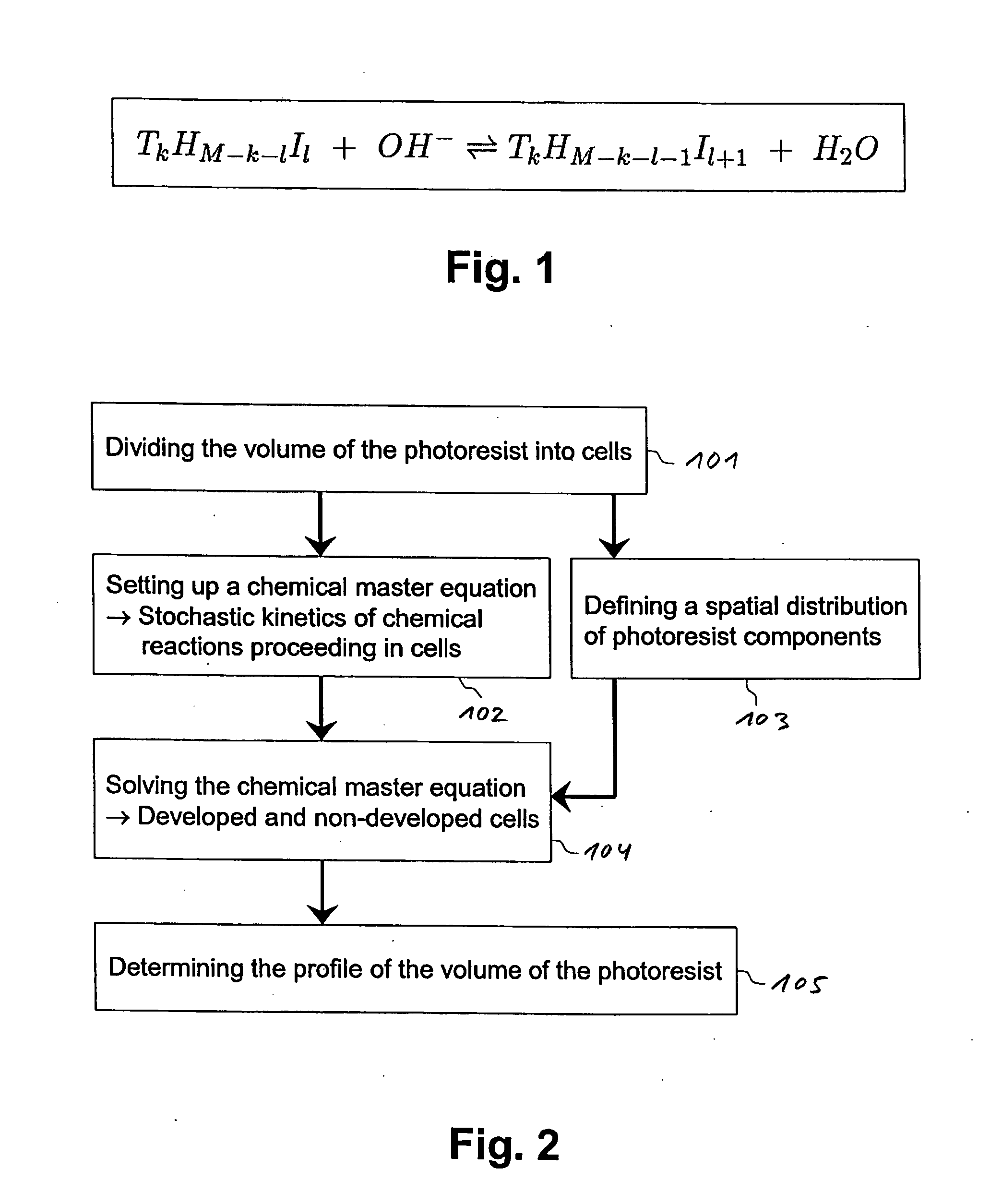
[0046]FIG. 1 shows a typical reaction scheme for a polymer of a photoresist during a development process illustrating a reversible ionization reaction between the polymer and components of a developer solution which is an aqueous base. The poly...
PUM
 Abstract
Description
Claims
Application Information