Method for manufacturing light emitting diode package

a technology manufacturing methods, which is applied in the field of manufacturing methods of light emitting diodes (led) packages, can solve the problems of difficult and costly manufacturing of molds with elaborate rough patterns, difficult regulation of the rough pattern formation process, and low light extraction efficiency. to achieve the effect of increasing light extraction efficiency

Inactive Publication Date: 2007-09-13
SAMSUNG ELECTRONICS CO LTD
View PDF9 Cites 54 Cited by
  • Summary
  • Abstract
  • Description
  • Claims
  • Application Information

AI Technical Summary

Benefits of technology

[0010] The present invention has been made to solve the foregoing problems of the prior art and therefore an aspect of the present invention is to provide a method of manufacturing a Light Emitting Diode (LED) package which can increase light extraction efficiency at a surface of a light-transmitting resin part such as a resin encapsulant or a lens.

Problems solved by technology

That is, it has been confirmed that adjusting the refractive index does not have a significant effect of improving the light extraction efficiency, especially in the case of a side view type LED package.
However, this method is not suitable for the LED package (see FIG. 1) with a reflecting cup formed therein and renders it difficult to regulate the process of forming the rough pattern.
Especially, it is difficult and costly to fabricate a mold with an elaborate rough pattern.
Further, in the process of pressing the resin encapsulant into a stamper having a rough pattern or etching a stamper, the resin encapsulant can be greatly damaged, degrading the optical characteristics.

Method used


Image

  • Method for manufacturing light emitting diode package
  • Method for manufacturing light emitting diode package
  • Method for manufacturing light emitting diode package

Examples


examples

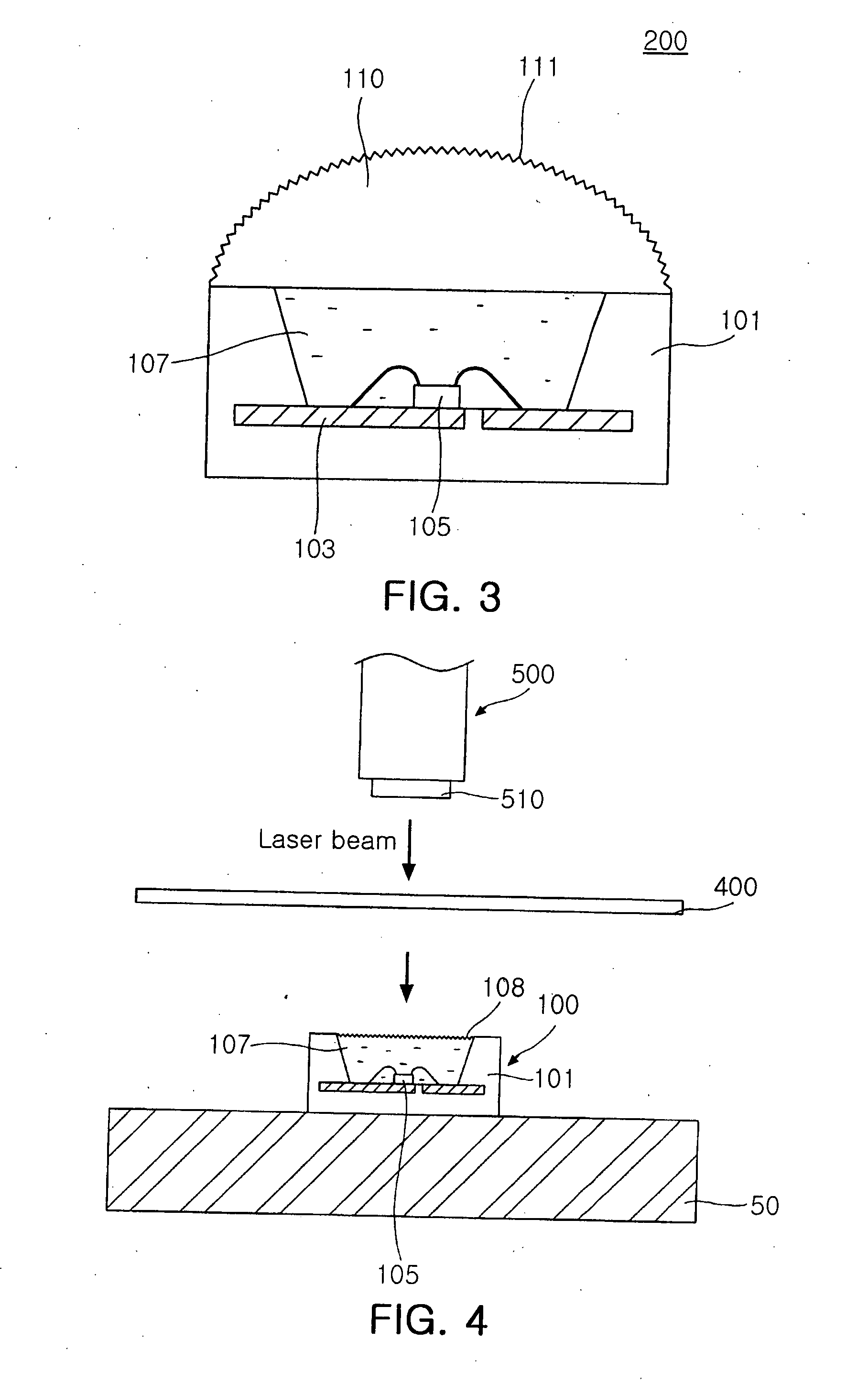
[0054] The inventors of the present invention conducted laser ablation on the surface of the silicone resin used for the resin encapsulant. The conditions for the laser ablation process were divided into two sets.

[0055] First, the LED chip was encapsulated by the silicon resin. Then, the silicone resin was dried and cured at 150° C. Using a KrF 248 nm excimer laser, the laser ablation was conducted under the following two sets of conditions on the cured silicone resin. [0056] (1) Beam power: 500 mJ / cm2, beam size: 1 mm×1 mm, repetition frequency: 100 Hz, pulse duration: tens of nanoseconds. [0057] (2) Beam power: 1000 mJ / cm2, beam size: 1 mm×1 mm, repetition frequency: 100 Hz, pulse duration: tens of nanoseconds.

[0058] Without conducting the laser ablation process, the surface of the cured silicone resin exhibited Average Roughness (Ra) of about 0.6 nm. However, after conducting the laser ablation under the conditions (1), it was confirmed that the surface of the silicone resin ex...


PUM


Abstract

A method of manufacturing an LED package with improved light extraction efficiency. A light-emitting resin part of an LED package is formed and laser beam is irradiated on a surface of the light-transmitting resin part of the LED package to roughen the surface thereof.

Description

CLAIM OF PRIORITY [0001] This application claims the benefit of Korean Patent Application No. 2006-0016848 filed on Feb. 21, 2006, in the Korean Intellectual Property Office, the disclosure of which is incorporated herein by reference. BACKGROUND OF THE INVENTION [0002] 1. Field of the Invention [0003] The present invention relates to a method of manufacturing a Light Emitting Diode (LED) package and, more particularly, to a method of manufacturing an LED package which can effectively improve light extraction efficiency. [0004] 2. Description of the Related Art [0005] Recently, Light Emitting Diodes (hereinafter, LEDs) have gained importance in various applications as an environmentally friendly light source which does not cause pollution. For example, the LEDs are applied to traffic lights, instruction lamps, keypads of mobile phones and the like, and also have proven their potential use as a backlight for LCD apparatuses or light sources for illumination. Such LEDs are combined wi...

Claims


Application Information

Patent Timeline
Patent Type & Authority Applications(United States)
IPC IPC(8): H01L21/00H01L33/22H01L33/54H01L33/56H01L33/60
CPCH01L2933/0091H01L33/54H01L2224/48247H01L2224/48257H01L2924/181H01L2924/00012A61B5/15003A61B5/150167A61M5/3287A61M5/3295A61M25/0606A61M25/065A61M39/0247A61M2039/0258
Inventor LEE, HAI SUNGLEE, JONG MYEONCHOO, HO SUNGCHANG, MYUNG WHUNPARK, YOUN GON
Owner SAMSUNG ELECTRONICS CO LTD
Why Eureka
Try Eureka