

Strained silicon with elastic edge relaxation
a technology of elastic edge relaxation and straining silicon, which is applied in the direction of semiconductor/solid-state device manufacturing, electrical apparatus, semiconductor devices, etc., can solve the problems of reducing channel mobility, reducing channel mobility, and not being introduced to cmos manufacturing
- Summary
- Abstract
- Description
- Claims
- Application Information
AI Technical Summary
Benefits of technology
Problems solved by technology
Method used
Image

Examples
Embodiment Construction
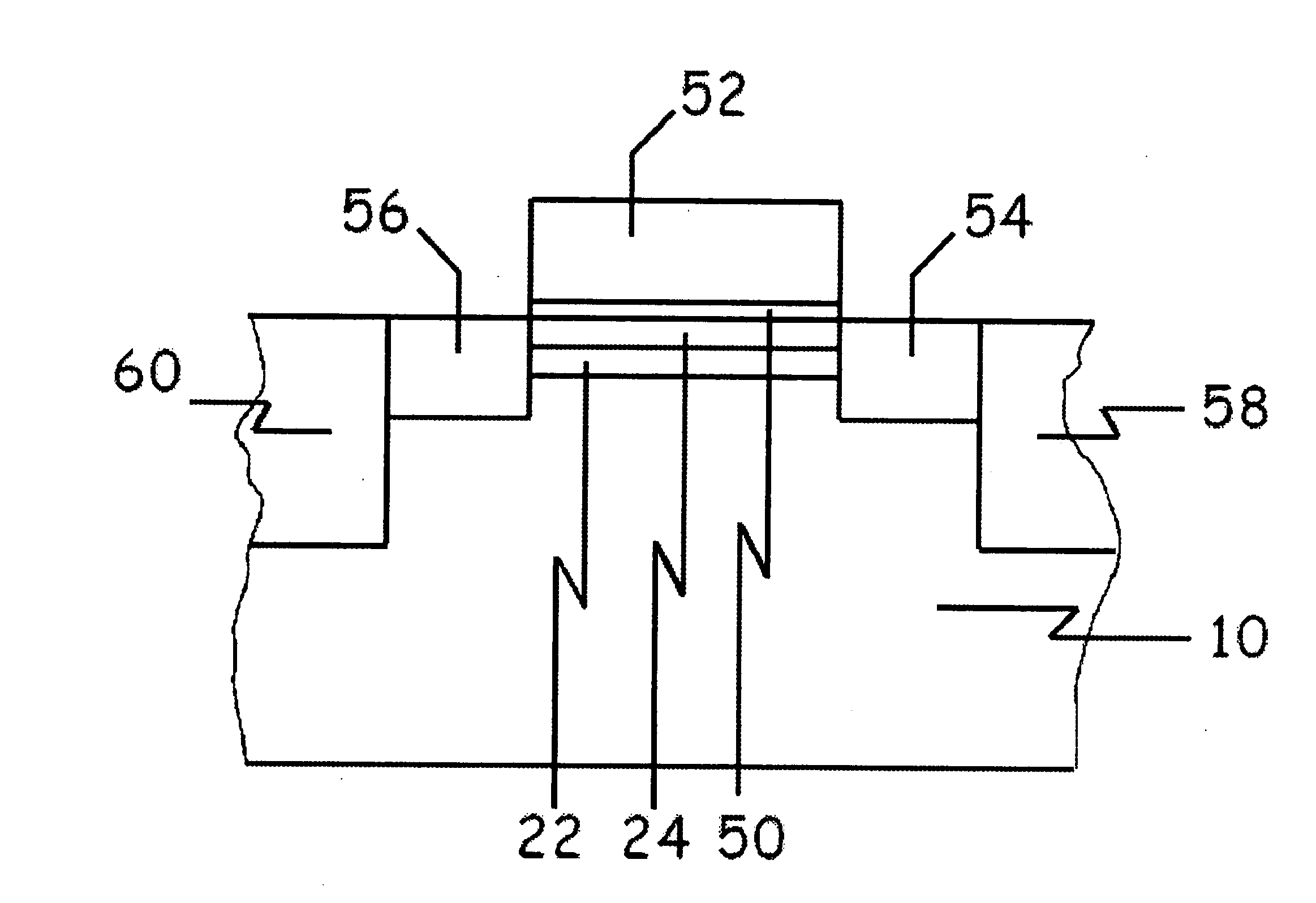
[0012] One aspect of the present invention provides a semiconductor device with a plurality of n-channel MOSFETs formed on a substrate. The substrate comprises silicon. Each of the n-MOSFET devices comprises a first layer comprising germanium formed over the substrate. The first layer has a thickness less than a first thickness at which misfit dislocations form in the first layer. The first layer has a first lower interface lattice spacing matched with a substrate interface lattice spacing characteristic of an interface region of the substrate. A second layer comprising silicon is formed over the first layer and the second layer has a second lower interface lattice spacing matched with a first layer upper interface lattice spacing characteristic of an upper interface of the first layer. A gate dielectric layer is provided on the second layer and separates the second layer from a gate electrode. A concentration of germanium in the first layer is greater than a concentration of german...
PUM
 Abstract
Description
Claims
Application Information