
Semiconductor device and method of manufacturing the same

a semiconductor and film technology, applied in the field of semiconductor devices, can solve the problems of affecting the performance of transistors, difficult implementation, and the speed at which the tcs-sin film is formed, and achieves the effect of reducing the cost of production, and improving the performance of the transistor

Inactive Publication Date: 2007-09-20
KK TOSHIBA
View PDF16 Cites 13 Cited by
  • Summary
  • Abstract
  • Description
  • Claims
  • Application Information

AI Technical Summary

Benefits of technology

[0003] The present invention relates to a semiconductor device and a manufacture method thereof, and in particular, to an insulating film provided in a semiconductor device.

Problems solved by technology

However, conventional SiN films formed using dichlorosilane (SiH2Cl2:DCS) may create various problems when they are used to manufacture next-generation semiconductor devices.
However, such measures may degrade the performance of the transistor and are thus difficult to implement.
However, the speed at which the TCS-SiN film is formed, is low and about one-third of that of the DCS-SiN film.
However, it is actually difficult to increase the film formation speed because of the need to keep the film uniform, prevent film quality from being degraded, suppress dusts, and the like.
Consequently, the use of the TCS-SiN film may reduce productivity.
A problem with the MONOS device is destruction of data resulting from write / erase stress.
Further, a problem with NAND type devices is destruction of data resulting from read stress.
Non-volatile memories need to retain charges for 10 years after writes / erases have been carried out 100,000 times. At present, however, data are not sufficiently retained.
However, this structure is not always optimum as described later.
However, the SiN film is a single layer formed using DCS or the like, and this structure is not always optimum.
However, this is not always optimum as described later.
This hinders data from being appropriately retained.
Consequently, this film cannot sufficiently retain data.
However, the use of TCS hinders the film formation speed from being increased, thus reducing productivity.
However, the corresponding conventional structure does not allow data to be sufficiently retained.

Method used


Image

  • Semiconductor device and method of manufacturing the same
  • Semiconductor device and method of manufacturing the same
  • Semiconductor device and method of manufacturing the same

Examples


embodiment 1

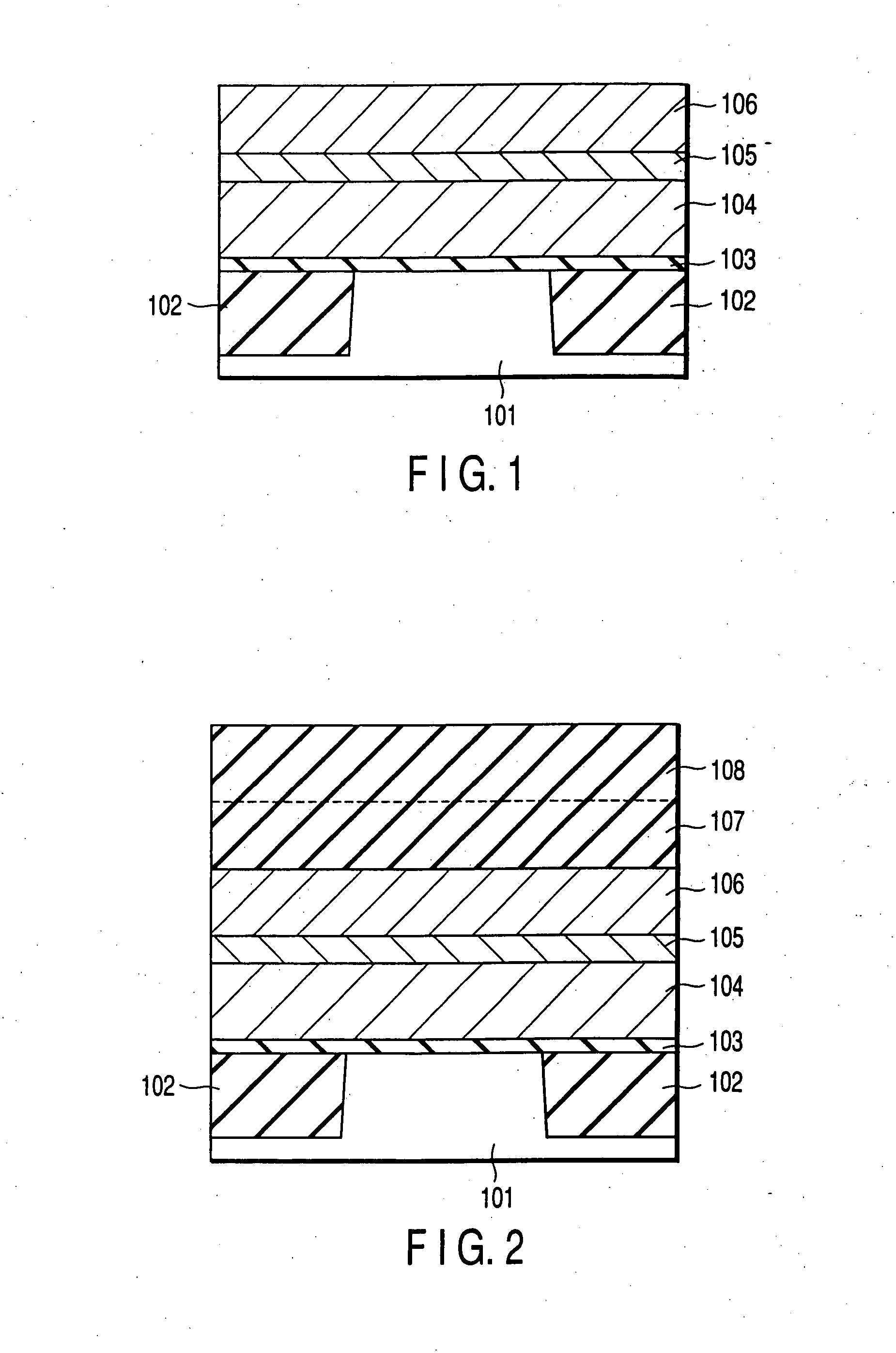
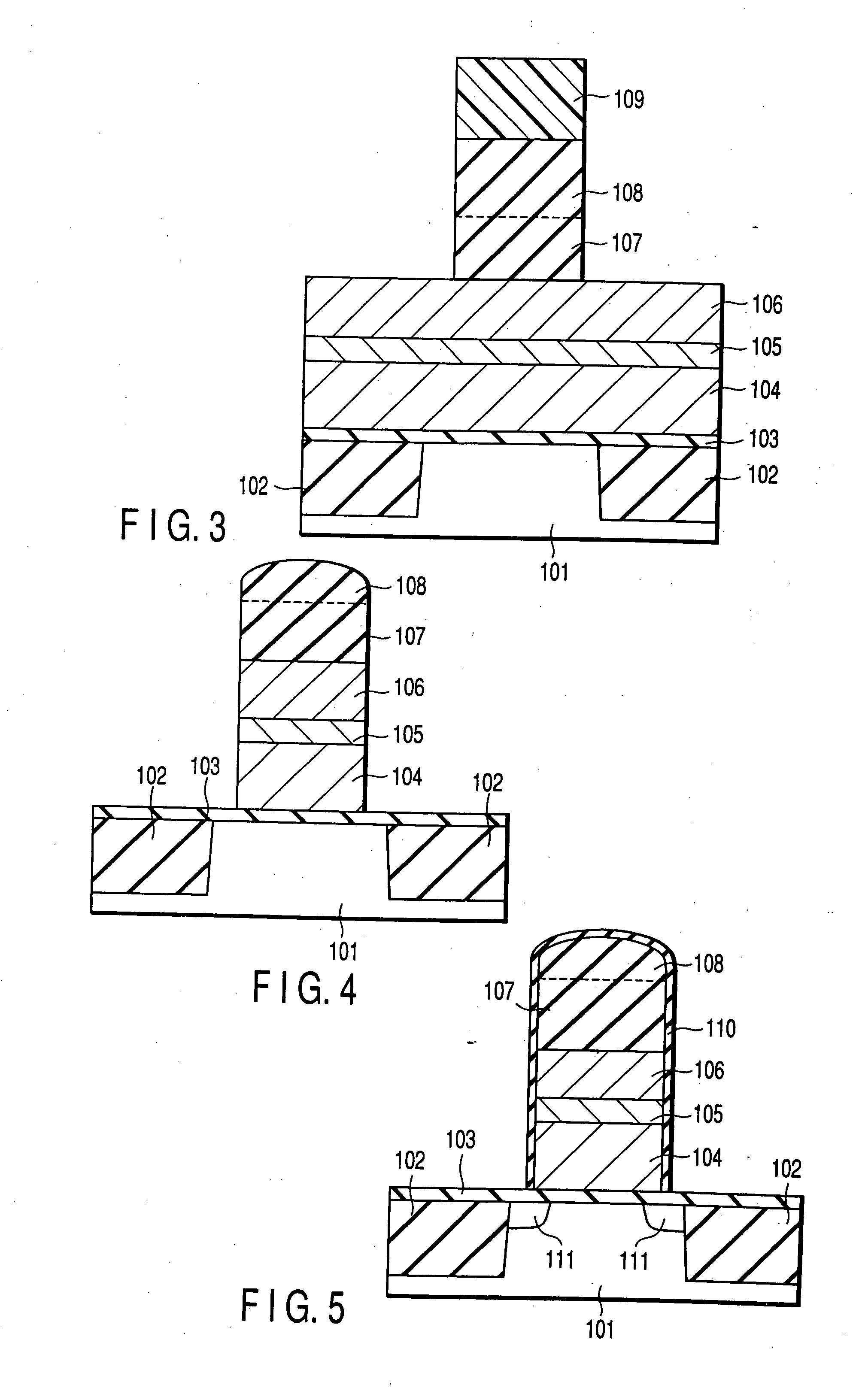
[0060] FIGS. 1 to 5 are sectional views showing a manufacture method for a semiconductor device (MIS transistor) according to a first embodiment of the present invention.

[0061] First, as shown in FIG. 1, an isolation region 102 and a gate insulating film 103 are formed on a silicon substrate 101. The gate insulating film 103 is a silicon oxynitride film of 4.5 nm thickness. Subsequently, a stacked structure composed of an amorphous silicon film 104 (70 nm), a tungsten nitride film 105 (5 nm), and a tungsten film 106 (40 nm) is formed on the gate insulating film 103 as a gate electrode. The amorphous silicon film 104 is doped with p-type impurities in a PMOS region and with n-type impurities in an NMOS region. For example, boron ions are implanted in the PMOS region at 5 keV over 5×10¹⁴ to 1×1016 cm−2, and phosphorous ions are implanted in the NMOS region at 10 keV over 5×10¹⁴ to 1×1016 cm−2. Thus, the amount of boron introduced into the PMOS gate electrode is more than 1×10¹⁹ / cm3 a...

embodiment 2

[0088] FIGS. 8 to 12 are sectional views showing a manufacture method for a semiconductor device (MIS transistor) according to a second embodiment of the present invention.

[0089] First, as shown in FIG. 8, the following components are formed on a silicon substrate 121 using a normal method: an isolation region (not shown), a gate insulating film 124, a gate electrode 125, a side wall insulating film 126, an extension region 123, and a source / drain region 122. The gate electrode 125 is formed of an amorphous silicon film. The amorphous silicon film is doped with p-type impurities in a PMOS region and with n-type impurities in an NMOS region. The impurities are implanted in the amorphous silicon film simultaneously with the implantation of ions in the source / drain region 122. For example, boron ions are implanted in the PMOS region at 7 keV over 5×10¹⁴ to 1×1016 cm−2, and arsenic ions are implanted in the NMOS region at 65 keV over 5×10¹⁴ to 1×1016 cm−2. The side wall insulating film...

embodiment 3

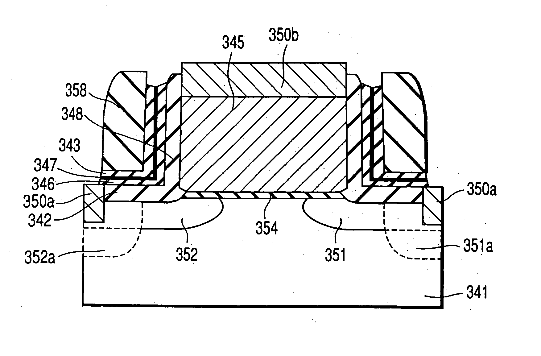
[0096]FIG. 13 is a sectional view showing the structure of a semiconductor device (a non-volatile memory or flash memory) according to a third embodiment of the present invention.

[0097] In FIG. 13, on a silicon substrate 141, the following components are formed: a tunnel insulating film 142, a floating gate 143 acting as a charge storage film, an inter-poly insulating film (an inter-electrode insulating film) 144, a control gate 145 formed of a polysilicon film, and a tungsten silicide film 146. Further, an SiN film 147 is formed on the tungsten silicide film 146, and an SiN film 148 is formed along side walls of a gate structure. At least one of the SiN film included in the inter-electrode insulating film 144, the SiN film 147, and the SiN film 148 has a stacked structure composed of a lower TCS-SiN film and an upper DCS-SiN film. Furthermore, source / drain diffusion layers 149 are formed so as to sandwich a gate structure.

[0098] This embodiment also produces effects similar to th...


PUM

PropertyMeasurementUnit
thicknessaaaaaaaaaa
thicknessaaaaaaaaaa
thicknessaaaaaaaaaa

Abstract

Disclosed is a semiconductor device comprising a semiconductor substrate, a gate electrode, a first insulating film formed between the semiconductor substrate and the gate electrode, and a second insulating film formed along a top surface or a side surface of the gate electrode and including a lower silicon nitride film containing nitrogen, silicon and hydrogen and an upper silicon nitride film formed on the lower silicon nitride film and containing nitrogen, silicon and hydrogen, and wherein a composition ratio N / Si of nitrogen (N) to silicon (Si) in the lower silicon nitride film is higher than that in the upper silicon nitride film.

Description

CROSS-REFERENCE TO RELATED APPLICATIONS [0001] This application is based upon and claims the benefit of priority from the prior Japanese Patent Application No. 2002-155740, filed May 29, 2002, the entire contents of which are incorporated herein by reference. BACKGROUND OF THE INVENTION [0002] 1. Field of the Invention [0003] The present invention relates to a semiconductor device and a manufacture method thereof, and in particular, to an insulating film provided in a semiconductor device. [0004] 2. Description of the Related Art [0005] Silicon nitride films (SiN films) are applied to various parts of a semiconductor device. However, conventional SiN films formed using dichlorosilane (SiH2Cl2:DCS) may create various problems when they are used to manufacture next-generation semiconductor devices. [0006] Possible problems with a next-generation DRAM employing a dual gate will be described by way of example. In a next-generation DRAM, a thick SiN film of about 200 nm thickness is used...

Claims


Application Information

Patent Timeline
Patent Type & Authority Applications(United States)
IPC IPC(8): H01L29/94H01L21/283H01L21/28H01L21/285H01L21/314H01L21/318H01L21/336H01L21/60H01L21/768H01L21/8242H01L21/8247H01L27/108H01L27/115H01L29/41H01L29/423H01L29/49H01L29/51H01L29/78H01L29/788H01L29/792
CPCH01L21/28176H01L21/28202H01L21/28247H01L21/28282H01L21/28518H01L21/3185H01L29/792H01L21/76897H01L29/513H01L29/518H01L29/665H01L29/6656H01L29/6659H01L21/76838H01L29/40117H01L21/022H01L21/0217G02F1/133528G02F1/1303
Inventor TANAKA, MASAYUKIOZAWA, YOSHIOSAIDA, SHIGEHIKOGODA, AKIRANOGUCHI, MITSUHIROMITANI, YUICHIROTSUNASHIMA, YOSHITAKA
Owner KK TOSHIBA
Learn More