Method for forming tantalum nitride film

A technology of nitride film and film forming chamber, which is applied in the direction of gaseous chemical plating, coating, electrical components, etc., can solve problems such as film difficulties, and achieve good adhesion and smoothness

Active Publication Date: 2007-12-19
ULVAC INC
View PDF1 Cites 0 Cited by
  • Summary
  • Abstract
  • Description
  • Claims
  • Application Information

AI Technical Summary

Problems solved by technology

[0007] In the case of the prior art described above, there is a problem that it is difficult to form a low-resistance tantalum nitride (TaN) film useful as a barrier film while ensuring adhesion with the Cu wiring film by the CVD method.

Method used


Image

  • Method for forming tantalum nitride film
  • Method for forming tantalum nitride film

Examples


Embodiment 1

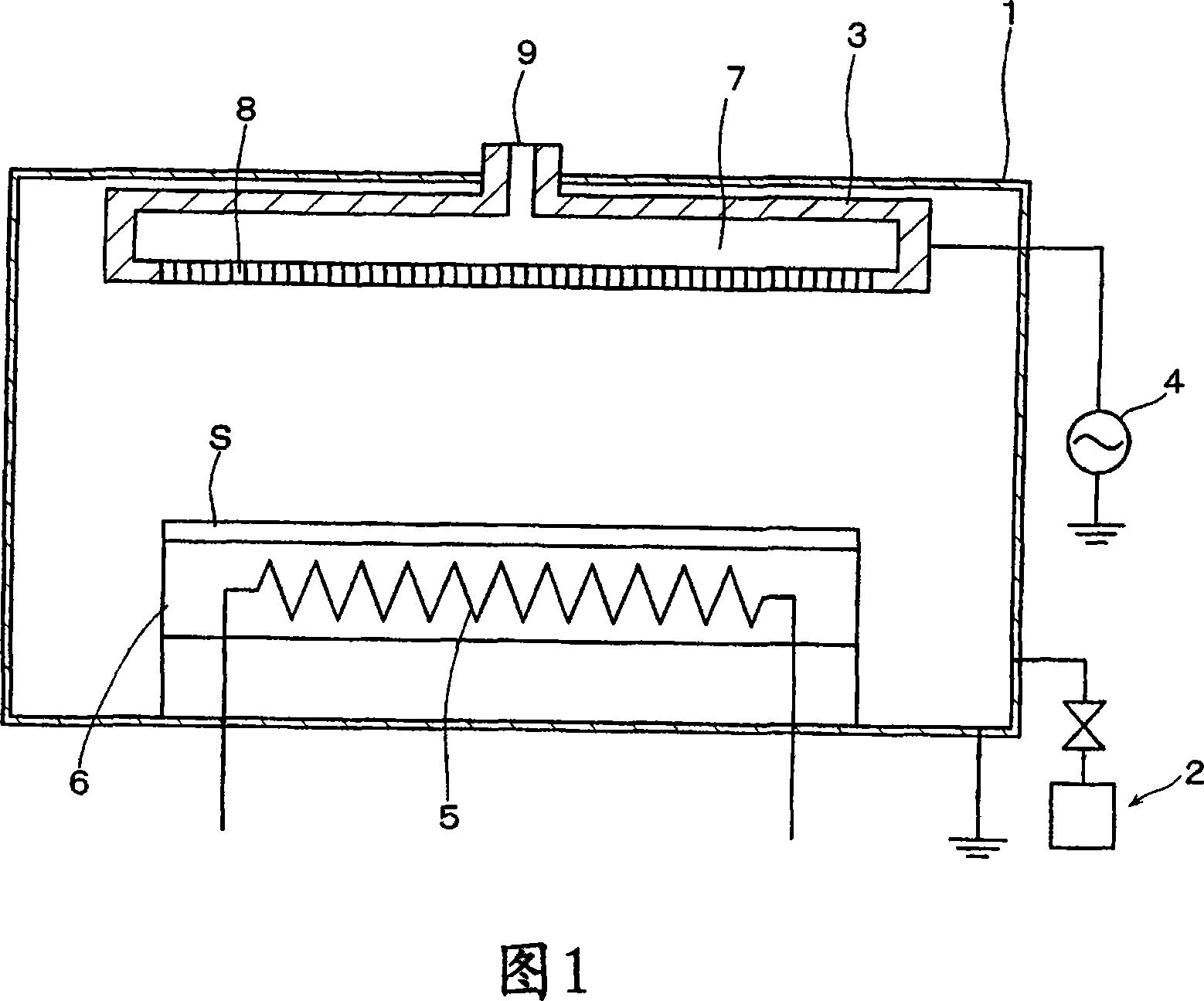
[0064] In this example, using the film forming apparatus 1 shown in FIG. 3 gas to form a tantalum nitride film.

[0065] According to known methods, in the implementation with SiO 2 After the degassing pretreatment process on the surface of the substrate S of the insulating film, the substrate S is moved into the vacuum exhaust system 2 to 10 -5 In the vacuum chamber 1 below Pa. The substrate is not particularly limited, and for example, a substrate in which plasma is generated by applying a voltage to a target mainly composed of Ta using Ar sputtering gas according to a common sputtering film formation method can also be used. , a sputtering target, a substrate on which a substrate-side adhesive layer is formed on the surface.

[0066] The substrate S is loaded into the vacuum chamber 1, and after the substrate S is placed on the substrate mounting table 6, the substrate is heated to 250° C. with the heater 5, and the gas introduction system 9 is introduced into the gas ch...

Embodiment 2

[0078] In this example, the tantalum nitride film obtained in Example 1 was implanted with tantalum particles by sputtering using a known sputtering device to form a tantalum nitride film further enriched in tantalum.

[0079] Ar sputtering gas is introduced into the sputtering device, a voltage is applied to the target from the voltage applying device to discharge, plasma is generated, and the target mainly composed of tantalum is sputtered, and incident on the thin film formed on the substrate S as sputtering. Tantalum particles that shoot particles. The sputtering conditions are DC power: 5kW, RF power: 600W. In addition, the sputtering temperature is -30 to 150°C.

[0080] The content of tantalum in the barrier film can be further increased by sputtering with implanted tantalum particles, and a desired low-resistance tantalum-rich tantalum nitride film can be obtained. In addition, by injecting tantalum into the surface thin film of the substrate S, the decomposition of ...

Embodiment 3

[0084] In addition to using t-amyliminotris(dimethylamino)tantalum instead of penta(dimethylamino)tantalum as the raw material gas, when the film-forming process was carried out according to Example 1, a tantalum-rich low Resistor with tantalum nitride film. For the obtained film, Ta / N=1.8, C content: 3%, N content: 35.7%, and resistivity 550 μΩ·cm.


PUM

PropertyMeasurementUnit
Resistivityaaaaaaaaaa

Abstract

According to a CVD method, a raw material gas composed of a coordinate compound in which an N=(R,R') group (wherein R and R' may be the same as or different from each other and respectively represent an alkyl group having 1-6 carbon atoms) is coordinated to a Ta element and a halogen gas are introduced into a film formation chamber for forming a TaNx(Hal)y(R,R')z compound film (wherein Hal represents a halogen atom), and then an H atom-containing gas is introduced therein and reacted with the halogenated product for forming a tantalum-rich tantalum nitride film. By this method, a low-resistance tantalum nitride film having low C and N contents, high Ta / N ratio and secure adhesion to a Cu film can be obtained, and this tantalum nitride film is useful as a barrier film. By implanting tantalum particles into the thus-obtained film by sputtering, there can be obtained a still tantalum-richer film.

Description

technical field [0001] The present invention relates to a method for forming a tantalum nitride film, and more particularly, to a method for forming a tantalum nitride film useful as a barrier film for wiring films by a CVD method. Background technique [0002] In recent years, the demand for microfabrication in the thin-film manufacturing technology in the semiconductor field has been accelerated, and various problems have arisen accordingly. [0003] For example, in the case of thin-film wiring processing in semiconductor devices, copper is mainly used as a wiring material due to low resistivity and other reasons. However, since copper is difficult to etch and diffuses easily in the insulating film of the base layer, there is a problem that the reliability of the device is low. [0004] In order to solve this problem, conventionally, a metal thin film (ie, a conductive barrier film) is formed on the inner wall surface of an interlayer connection hole in a multilayer wirin...

Claims


Application Information

Patent Timeline
IPC IPC(8): C23C16/34H01L21/3205H01L21/285H01L23/52
CPCC23C16/34H01L21/28556H01L2924/0002H01L21/76859H01L21/76843H01L23/53238H01L2924/00H01L21/285H01L23/52
Inventor 五户成史丰田聪牛川治宪近藤智保中村久三
Owner ULVAC INC
Why Eureka
Try Eureka