Substrate transporting and processing apparatus, fault management method for substrate transport and processing apparatus, and storage medium storing fault management program

a substrate and processing apparatus technology, applied in the direction of instruments, computing, electric digital data processing, etc., can solve the problems of affecting resist pattern, affecting product yield rate, so as to avoid increase in time interval and reduce product yield rate

Inactive Publication Date: 2007-09-20
TOKYO ELECTRON LTD
View PDF1 Cites 28 Cited by
  • Summary
  • Abstract
  • Description
  • Claims
  • Application Information

AI Technical Summary

Benefits of technology

[0010] The present invention makes it possible to avoid increase in the time interval from the exposure process completion

Problems solved by technology

However, if a substrate transport operation is delayed in a resist coating and developing apparatus, the resulting resist pattern may be adversely affected.
In a case where a chemically-amplified resist is used, the time from an exposure process to a post-exposure baking process must be fixed, oth

Method used


Image

  • Substrate transporting and processing apparatus, fault management method for substrate transport and processing apparatus, and storage medium storing fault management program
  • Substrate transporting and processing apparatus, fault management method for substrate transport and processing apparatus, and storage medium storing fault management program
  • Substrate transporting and processing apparatus, fault management method for substrate transport and processing apparatus, and storage medium storing fault management program

Examples


case 1

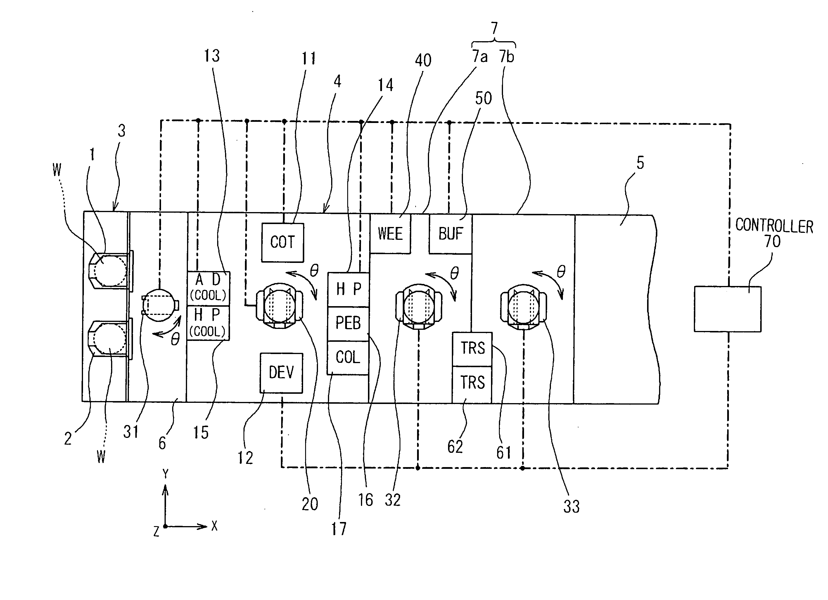
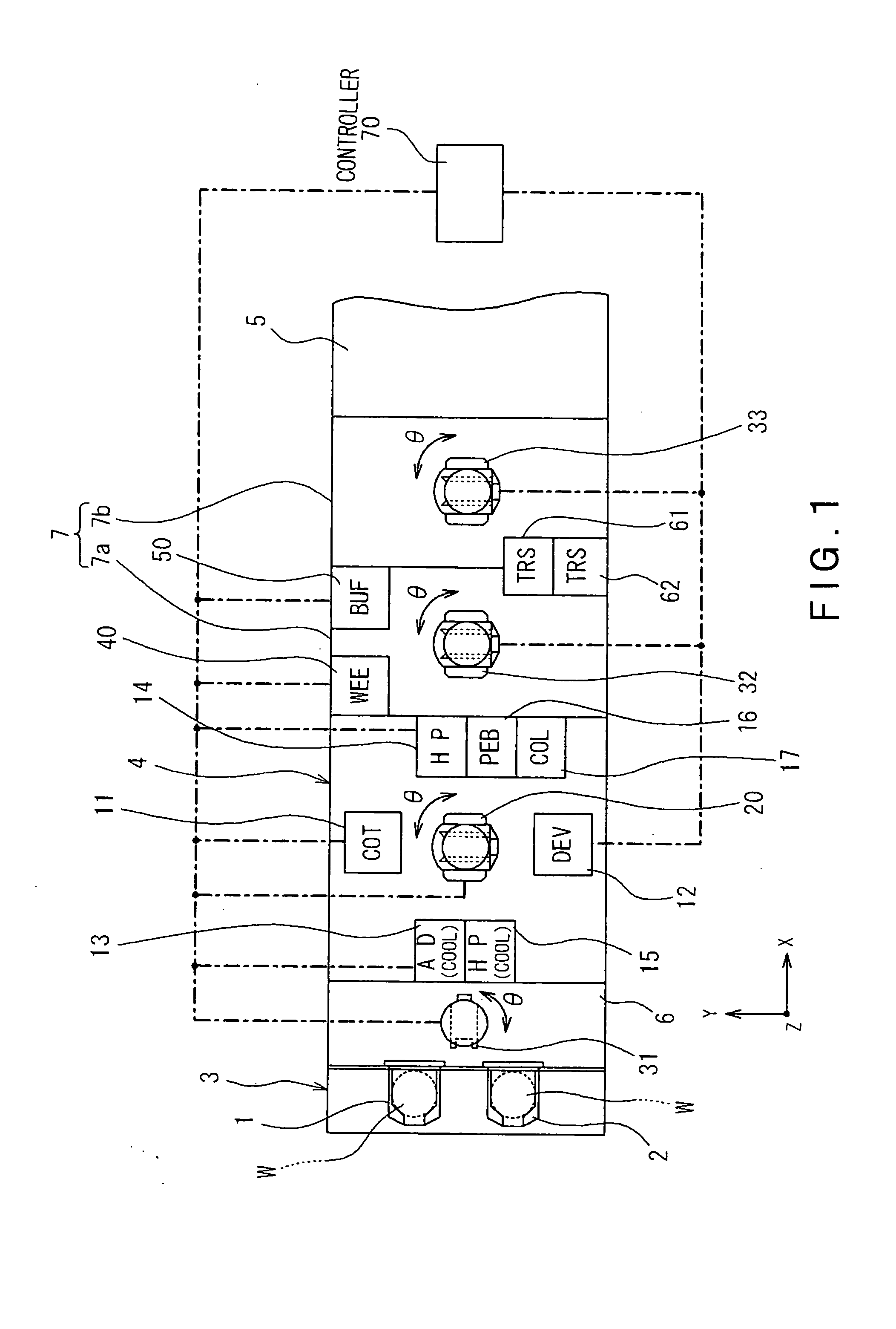
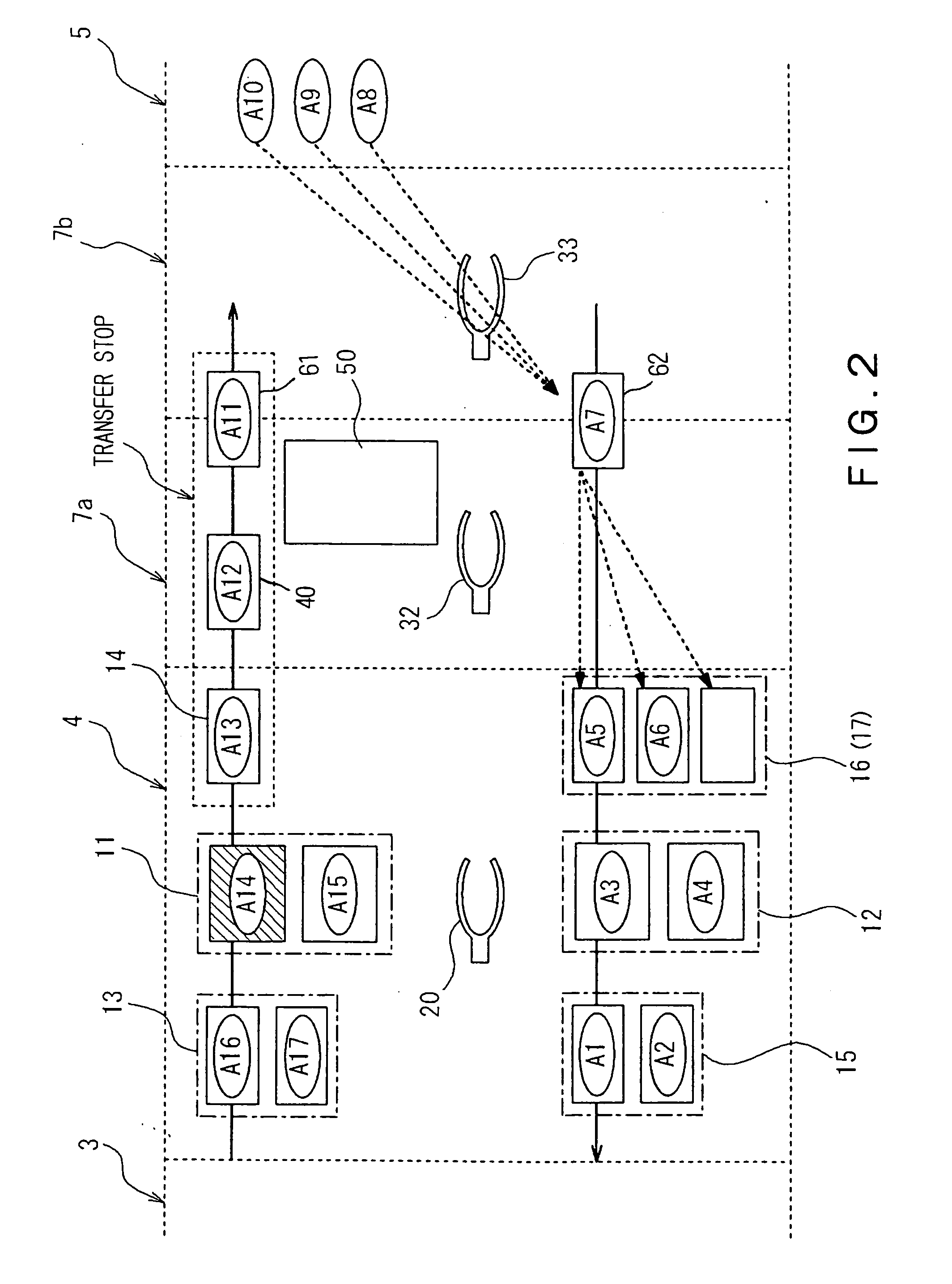
[0036] (Case 1) A fault that occurs in a process module (e.g., developing module 12 or second hot plate module 15) positioned downstream of a process module for performing a PEB process in the post-exposure substrate transport path;

case 2

[0037] (Case 2) A fault that occurs in a transport module (i.e., the main transport module 20) for loading or unloading a substrate into or from a process module positioned downstream of a process module for performing the PEB process in the post-exposure substrate transport path; and

case 3

[0038] (Case 3) A fault that occurs in a process module (e.g., the adhesion module 13, the coating module 11, or the first hot plate module 14) located in a pre-exposure substrate transport path (i.e., a wafer transport path from the cassette 1 to the exposure apparatus 5), the loading and unloading of a substrate into and from which is assigned to a transport module (i.e., the main transport module 20) that also takes charge of the loading and unloading of a substrate into and from a process module positioned downstream of a process module for performing the PEB process in the post-exposure substrate transport path.

[0039] Case 3 corresponds to “a fault of a process module or transport module that makes it impossible to transport a substrate to a process module positioned downstream of a process module for performing a PEB process”, because the main transport module 20 in this embodiment can perform only a transport operation in accordance with a predetermined transport schedule (he...


PUM


Abstract

Disclosed is a countermeasure to be taken when a fault occurs in one of process modules 11-17 or a transport module 20 that makes it impossible to transport substrates to a process module positioned downstream of a post-exposure baking module 15 in accordance with a predetermined transport schedule in a post-exposure substrate transport path that starts from an exposure apparatus 5 and goes through the post-exposure baking (PEB) module 15, a developing module 12, and a post-development baking module 15. In this instance, part of post-exposure processes to a post-exposure baking process are continuously performed to the exposed substrates and the wafers W having been subjected to the PEB process are loaded into a buffer module 32 and temporarily stored in the buffer module 32 until the fault is cleared. This prevents increase in the time period from an exposure process completion to the post-exposure baking process even when the fault occurs, thereby avoiding defective line width the circuit pattern of a resist, particularly a chemically amplified resist.

Description

TECHNICAL FIELD [0001] The present invention relates to a substrate transporting and processing apparatus that includes plural sorts of process modules, which perform predetermined pre-exposure processes or post-exposure processes to a substrate, such as a semiconductor wafer or an LCD glass substrate, and a transport system, which has at least one transport module for transporting the substrate between the process modules. More particularly, the present invention relates to countermeasures against a fault which may occur in any one of the modules and which might adversely affect the substrate quality BACKGROUND ART [0002] In processing of a substrate such as a semiconductor wafer or a LCD (Liquid Crystal Display) substrate, photolithography technique is generally employed to form an ITO (Indium Tin Oxide) thin film and an electrode pattern on the substrate. Photolithography includes a process for applying a photoresist to the substrate, a process for exposing a resist, a process fo...

Claims


Application Information

Patent Timeline
IPC IPC(8): G06F19/00H01L21/027H01L21/677
CPCH01L21/67745H01L21/67271H01L21/67155H01L21/6719H01L21/67196H01L21/67225H01L21/67742
Inventor KANEKO, TOMOHIROMIYATA, AKIRA
Owner TOKYO ELECTRON LTD
Why Eureka
Try Eureka