
Watermarking Apparatus, Software Enabling an Implementation of an Electronic Circuit Comprising a Watermark, Method for Detecting a Watermark and Apparatus for Detecting a Watermark

a technology of electronic circuits and watermarks, applied in the field of watermarking integrated circuits, can solve the problems of lack of protection against unlicensed use, short product cycle, and inability of common tools to handle encrypted cores, and achieve the effect of efficient detection

Active Publication Date: 2007-09-20
FRAUNHOFER GESELLSCHAFT ZUR FOERDERUNG DER ANGEWANDTEN FORSCHUNG EV +1
View PDF0 Cites 29 Cited by
  • Summary
  • Abstract
  • Description
  • Claims
  • Application Information

AI Technical Summary

Benefits of technology

[0019]It is an object of the present invention to provide a watermarking apparatus and a software for enabling an implementation of an electronic circuit comprising a watermark, wherein the watermark can be efficiently detected by only analyzing the electronic circuit and to provide a method and an apparatus for detecting said watermark of said electronic circuit.
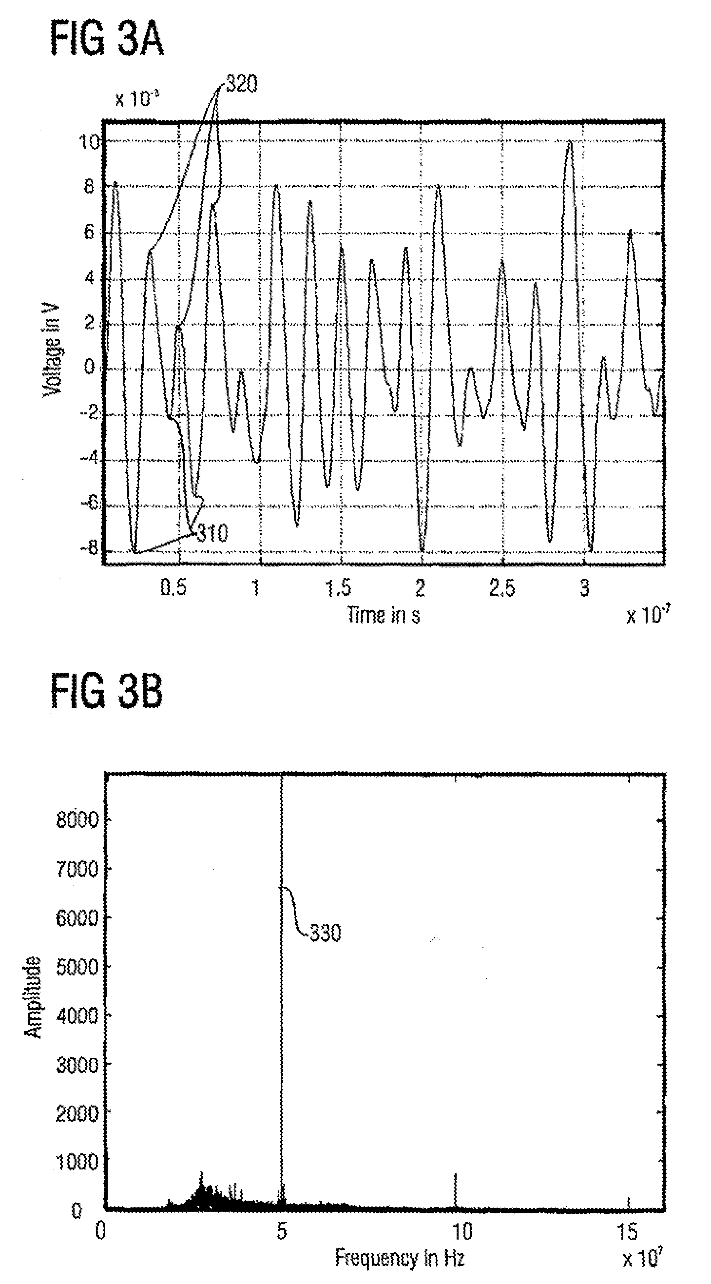
[0028]In preferred embodiments of the present inventions the watermarking apparatus generates a watermarking signal based on said watermark, wherein the watermarking signal is a voltage signal applied to a power supply line. Thus, the watermarking signal can be measured, for example, at the power supply pins or contacts of said electronic circuit. The watermarking signal can be measured on said electronic circuit without the need of further hardware, like the PROM or further information from a third party. Thus, the verification and proof of the existence of the watermark can be efficiently performed at any time.
[0030]The invention is explained based on an embodiment, where FPGA cores are watermarked and where the signature (watermark) is detected at the power supply pins of the FPGA. This is the first watermarking method, where the signature is extracted in this way. One is now able to watermark cores at the netlist as well as the bitfile level, so a wide spectrum of cores can be watermarked. Embodiments of the power watermarking methods work with all types of FPGAs, but with Xilinx FPGAs, the watermarking algorithms and the signature can be integrated into the functionality of the watermarked core. Thus, it is very hard to remove the watermark without destroying the core. A detection algorithm is introduced, which can decode the signature from a voltage trace with high probability. Additionally, a second algorithm based on spreading the watermark is introduced, which improves the detection probability in case of considerable noise sources. Using this latter algorithm, it is possible to decode the signature even if other cores operate on the same device at the same time.

Problems solved by technology

On the other hand, the market requires shorter product cycles.
One problem of the distribution of IP cores is the lack of protection against unlicensed usage.
The disadvantage is that common tools cannot handle encrypted cores and that the shipped tools can be modified.
But most of these concepts are not applicable due to the lack of verification capabilities.
The major drawback of these approaches are the limitations of the verification possibilities of the watermarked core.
Monitoring the communication between PROM and FPGA in this case is useless, because only the encrypted file will be transmitted.
Also the introduced approaches at the HDL (Hardware Description Language) and netlist-levels turn out not to be applicable due to the lack of verification possibilities.
Thus, it can be summarized that the aforementioned approaches for inserting watermarks to FPGAs add overhead, e.g. additional elements not used for the normal operation of the integrated circuit, or limit the optimization of the integrated circuits due to constraints used for watermarking or identification of these integrated circuits.
The major disadvantage of the aforementioned approaches are the limited possibilities to detect whether the integrated circuit has a watermark and if the integrated circuit has a watermark, to identify which watermark this particular integrated circuit has.
These approaches, for example, all lack the possibility to detect a watermark by only analyzing the specific integrated circuit, for example, a FPGA or an ASIC or a specific IP core on one of the aforementioned integrated circuits.

Method used


Image

  • Watermarking Apparatus, Software Enabling an Implementation of an Electronic Circuit Comprising a Watermark, Method for Detecting a Watermark and Apparatus for Detecting a Watermark
  • Watermarking Apparatus, Software Enabling an Implementation of an Electronic Circuit Comprising a Watermark, Method for Detecting a Watermark and Apparatus for Detecting a Watermark
  • Watermarking Apparatus, Software Enabling an Implementation of an Electronic Circuit Comprising a Watermark, Method for Detecting a Watermark and Apparatus for Detecting a Watermark

Examples


Embodiment Construction

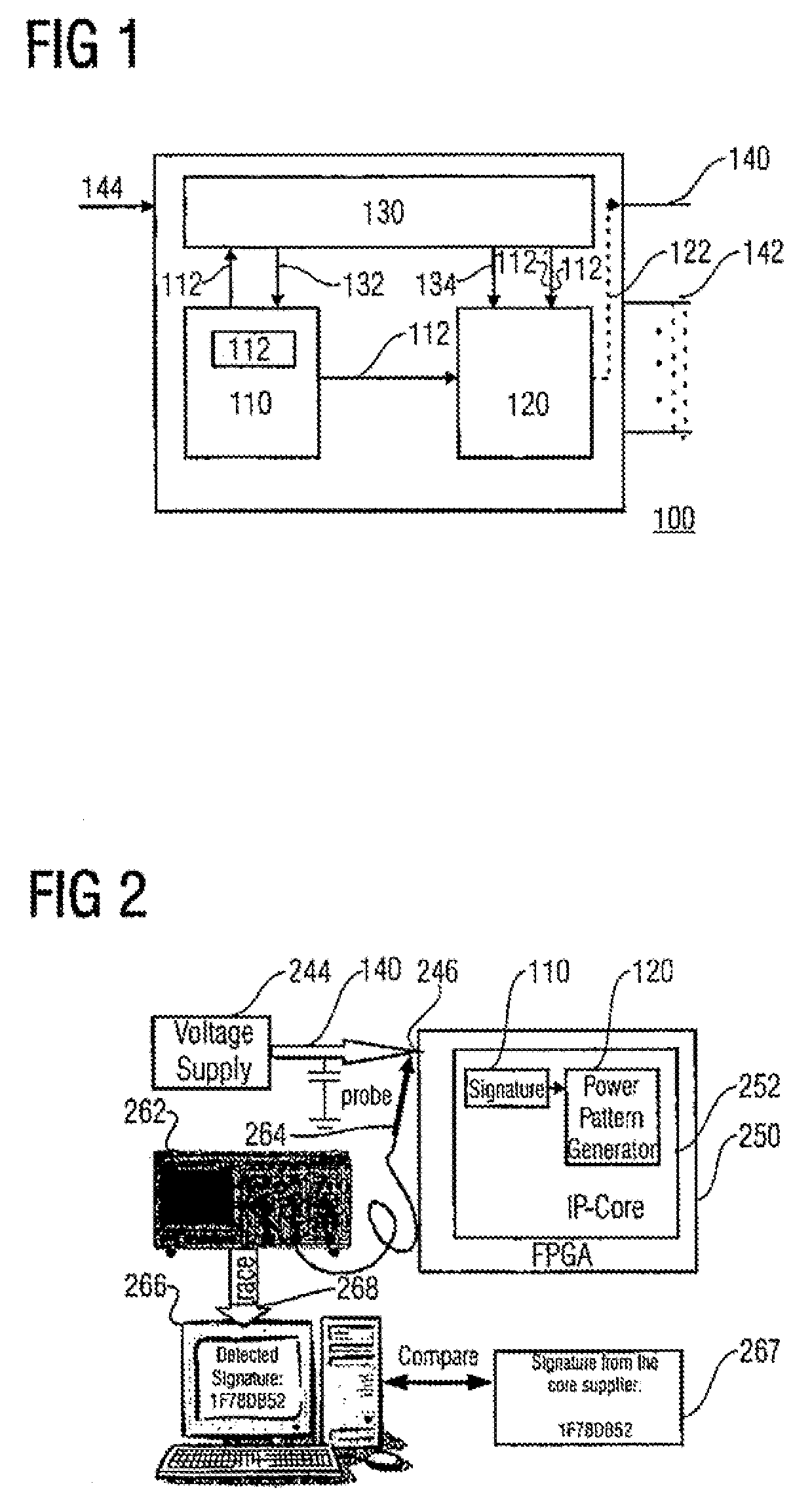
[0049]FIG. 1 shows a preferred embodiment of an inventive watermarking apparatus 100 for an electronic circuit comprising a watermark memory 110, a watermarking signal generator 120 and a watermarking signal control 130.

[0050]Said watermark memory is operative to store a watermark, characterizing said electronic circuit. Said watermarking signal generator 120 is operative to generate based on said watermark 112 stored in said watermark memory 110, the watermarking signal 122 detectable for a detection of said watermark 112 on a power supply line 140 of said electronic circuit 100.

[0051]The watermarking signal 122 detectable on said power supply line 140 is shown in broken lines to distinguish it from other signal paths used for transmitting, for example, data to or on data pins 142.

[0052]The watermark memory 110 can be operative to output the watermark 112 at once as a binary or any other value or to output the watermark 112 as a sequence of values, for example, a sequence of Bits.

[...


PUM


Abstract

A watermarking apparatus for an electronic circuit is described, which comprises the following features: a watermark memory operative to store a watermark characterizing said electronic circuit, and a watermarking signal generator operative to generate based on said watermark a watermarking signal on a power supply line of said electronic circuit, wherein said watermarking signal is detectable for a recognition of said watermark.

Description

CROSS-REFERENCE TO RELATED APPLICATION[0001]This application claims priority from European Patent Application No. 0600526.6, which was filed on Mar. 17, 2006, and is incorporated herein by reference in its entirety.BACKGROUND OF THE INVENTION[0002]1. Field of the Invention[0003]The present invention relates to the field of watermarking electronic circuits and, in particular, to the watermarking of integrated circuits, like FPGA (field programmable gate arrays) or ASIC (application specific integrated circuits) designed based on IP cores (Intellectual Property cores).[0004]2. Description of Related Art[0005]In the 1970s, only basic functions like discrete logical gates were implemented on integrated circuits. With improvements in the chip manufacturing, the size of the transistors was drastically reduced and the maximum size of a die was increased as well. Now it is possible to integrate one billion transistors on one chip, as described bys Xilinx, Inc., “Next-Generation Virtex Famil...

Claims


Application Information

Patent Timeline
IPC IPC(8): H04L9/00G06F21/73G06F21/76G06F21/81
CPCG06F17/5045G06F21/81G06F21/76G06F21/73G06F30/30
Inventor ZIENER, DANIELTEICH, JUERGEN
Owner FRAUNHOFER GESELLSCHAFT ZUR FOERDERUNG DER ANGEWANDTEN FORSCHUNG EV
Learn More