
Nonvolatile semiconductor memory device

Inactive Publication Date: 2007-09-27
SEMICON ENERGY LAB CO LTD
View PDF49 Cites 25 Cited by
  • Summary
  • Abstract
  • Description
  • Claims
  • Application Information

AI Technical Summary

Benefits of technology

[0009]As for the gate insulating layer provided between the floating gate and the semiconductor substrate, the thickness thereof is required to be small sequentially to inject charges to the floating gate by a low voltage. On the other hand, in order to hold charges stably for a long period of time, the thickness thereof is required to be large so that charge leakage or impurity penetration is prevented.
[0010]After all, the conventional nonvolatile memory requires a high writing voltage, and ensures the reliability against degradation of a charge holding property due to a repeat of writing, by performing a treatment such as error detection and error correction with a redundant memory cell provided or a controller devised.
[0011]In view of the foregoing, it is an object of the present invention to provide a nonvolatile semiconductor memory device which is superior in writing property and charge holding property.
[0017]When a floating gate is formed over a semiconductor substrate with a first insulating layer which functions as a tunnel insulating layer interposed therebetween, by forming the floating gate of a semiconductor material at least containing germanium, it becomes easy to inject charges from the channel formation region in the semiconductor substrate to the floating gate, and a charge holding property in the floating gate can be improved.
[0018]Further, by forming the floating gate of a material having similar characteristics to those of silicon, a nonvolatile semiconductor memory device with superior properties can be manufactured without decrease in productivity. Germanium which is a material of Group 14 in the Periodic Table of the Elements that is the same as silicon and is a semiconductor enables microfabrication of a thin film without imposing a burden on a manufacturing apparatus.

Problems solved by technology

If such a state is formed, it becomes difficult to inject electrons from the semiconductor substrate to the floating gate, so that a writing voltage is required to be increased.

Method used


Image

  • Nonvolatile semiconductor memory device
  • Nonvolatile semiconductor memory device
  • Nonvolatile semiconductor memory device

Examples


embodiment mode 1

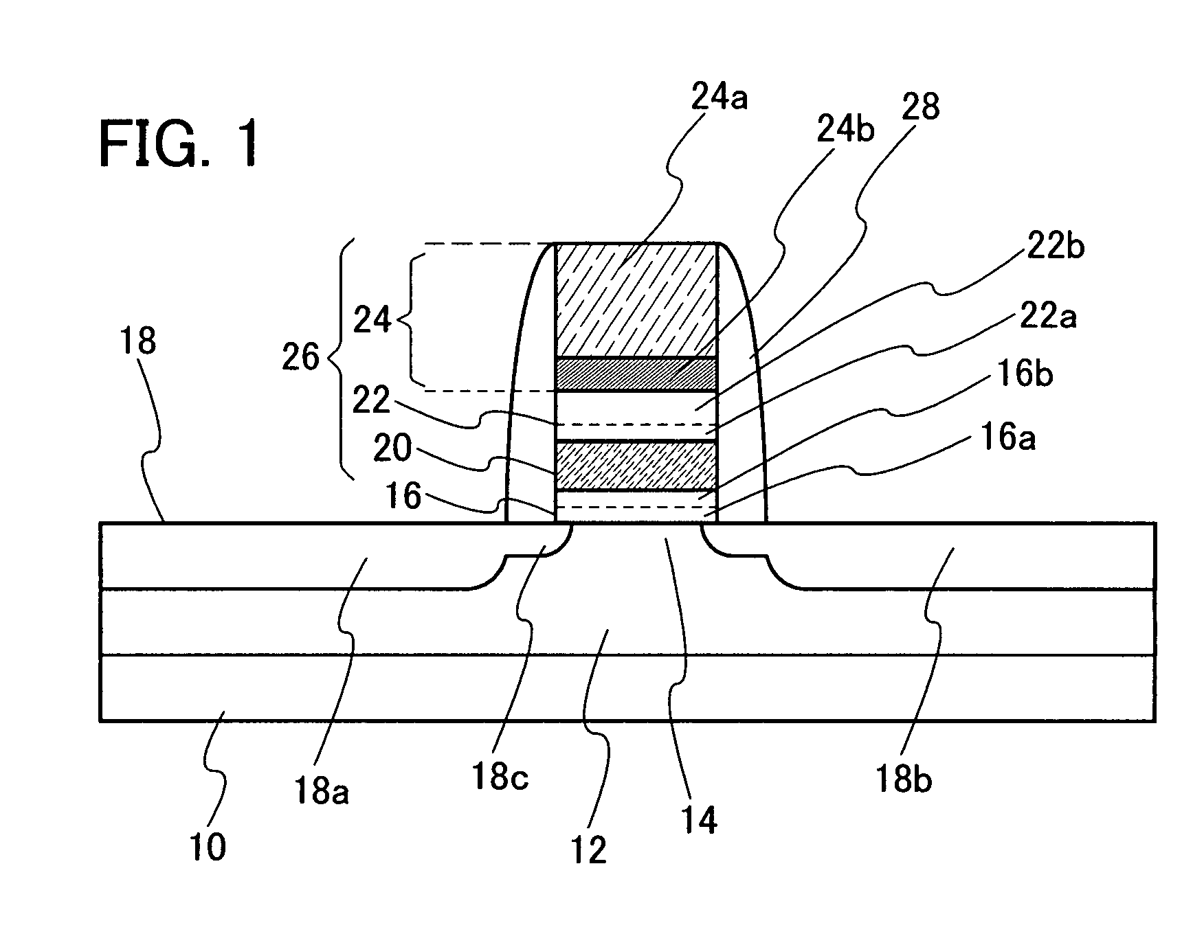
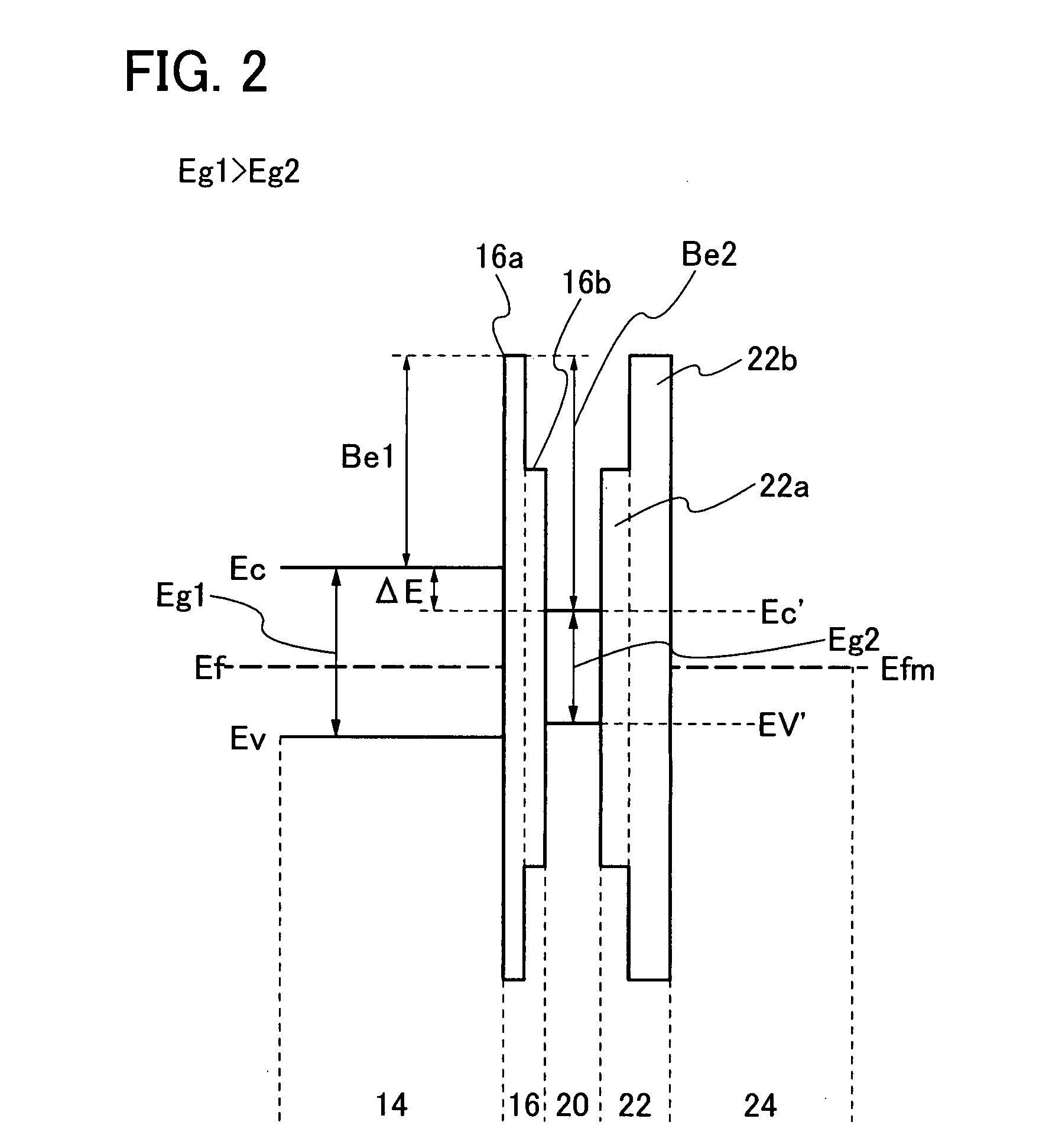
[0061]FIG. 1 is a cross-sectional diagram for describing a main structure of a nonvolatile semiconductor memory device of the present invention. FIG. 1 particularly illustrats a substantial part of the nonvolatile memory element. This nonvolatile memory element is manufactured using a semiconductor substrate 10. As the semiconductor substrate 10, a single crystalline silicon substrate (silicon wafer) is preferably used. Alternatively, an SOI (Si-On-Insulator) substrate can be used. As the SOI substrate, a so-called SIMOX (Separation by IMplanted Oxygen) substrate may be used which is manufactured by implanting oxygen ions into a mirror-polished wafer and then performing high-temperature annealing so that an oxide film layer is formed at a position with a certain depth from a top surface as well as a defect occurred in a top surface layer is vanished.

[0062]In the case where the substrate 10 is of an n-type, a p-well 12 into which a p-type impurity is injected is formed. As the p-type...

embodiment 1

[0118]This embodiment will describe one example of a nonvolatile semiconductor memory device with reference to the drawings. A description is made below on the case where a nonvolatile memory element for forming a memory portion is formed at the same time as an element such as a transistor for forming a logic portion that is provided over the same substrate as the memory portion and performs control of the memory portion or the like in a nonvolatile semiconductor memory device.

[0119]First, an equivalent circuit of a memory portion in the nonvolatile semiconductor memory device is shown in FIG. 8.

[0120]In the memory portion described in this embodiment, a plurality of memory cells each including a selecting transistor and a nonvolatile memory element is provided. In FIG. 8, one memory cell includes a selecting transistor S01 and a nonvolatile memory element M01. Similarly, each memory cell includes a selecting transistor S02 and a nonvolatile memory element M02, a selecting transisto...

embodiment 2

[0163]This embodiment will describe a manufacturing method of a nonvolatile semiconductor memory device, which is different from Embodiment 1, with reference to the drawings. The same ones as those in Embodiment 1 are denoted by the same reference symbols, and repeat description thereof is omitted. Note that in FIGS. 21A to 21C, 22A to 22C, and 23A and 23B, portions between A and B and between C and D illustrate transistors provided in a logic portion, a portion between E and F illustrates a nonvolatile memory element provided in a memory portion, and a portion between G and H illustrates a transistor provided in the memory portion. In addition, although description in this embodiment is made on the case where the transistor provided in the portion between A and B is of a p-channel type, the transistors provided in the portions between C and D and between G and H are of an n-channel type, and carrier movement of the nonvolatile memory element provided in the portion between E and F ...


PUM


Abstract

A nonvolatile semiconductor memory device which is superior in writing and charge holding properties, including a semiconductor substrate in which a channel formation region is formed between a pair of impurity regions formed with an interval, and a first insulating layer, a floating gate, a second insulating layer, and a control gate over an upper layer portion of the semiconductor substrate. It is preferable that a band gap of a semiconductor material forming the floating gate be smaller than that of the semiconductor substrate. For example, it is preferable that the band gap of the semiconductor material forming the floating gate be smaller than that of the channel formation region in the semiconductor substrate by 0.1 eV or more. This is because, by decreasing the bottom energy level of a conduction band of the floating gate electrode to be lower than that of the channel formation region in the semiconductor substrate, carrier injecting and charge holding properties are improved.

Description

BACKGROUND OF THE INVENTION[0001]1. Field of the Invention[0002]The present invention relates to a nonvolatile semiconductor memory device capable of electrical writing, reading, and erasing, and a manufacturing method thereof. In particular, the present invention relates to a structure of a floating gate in the nonvolatile semiconductor memory device.[0003]2. Description of the Related Art[0004]The market has been expanding for nonvolatile memories in which data can be electrically rewritten and data can be kept stored even after the power is turned off. Features of a nonvolatile memory are that its structure is similar to that of a MOSFET (Metal Oxide Semiconductor Field Effect Transistor) and a region capable of accumulating charges for a long period of time is provided over a channel formation region. This charge accumulation region which is formed over an insulating layer and is isolated and separated from the surround is also called a floating gate. Since the floating gate is ...

Claims


Application Information

Patent Timeline
IPC IPC(8): H01L29/788
CPCG11C16/0416G11C16/0433G11C16/0483H01L21/28273H01L29/7883H01L27/11526H01L27/11529H01L29/42324H01L29/66825H01L27/105H01L29/40114H10B41/40H10B41/41H01L21/02252
Inventor YAMAZAKI, SHUNPEIASAMI, YOSHINOBUTAKANO, TAMAEFURUNO, MAKOTO
Owner SEMICON ENERGY LAB CO LTD
Learn More