Memory device using quantum dots

Active Publication Date: 2007-09-27
SAMSUNG ELECTRONICS CO LTD
View PDF9 Cites 30 Cited by
  • Summary
  • Abstract
  • Description
  • Claims
  • Application Information

AI Technical Summary

Benefits of technology

[0010] Accordingly, embodiments of the present invention have been made keeping in mind the above problems occurring in the related art, and an object of embodimen

Problems solved by technology

However, conventional flash memory is disadvantageous because it may be recorded and erased a limited number of times and has a slow recording speed.
Further, in order to manufacture flash memory having a high memory capacity, line width per unit area should be decreased, which increases process costs resulting in high costs to manufacture memory chips.
Moreover, due to difficulties in chip manufacturing techniques it is difficult to further miniaturize the chips.
However, since the electroforming process cannot control the size or size distribution of metal p

Method used


Image

  • Memory device using quantum dots
  • Memory device using quantum dots
  • Memory device using quantum dots

Examples


example 1

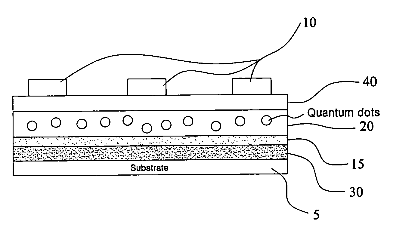
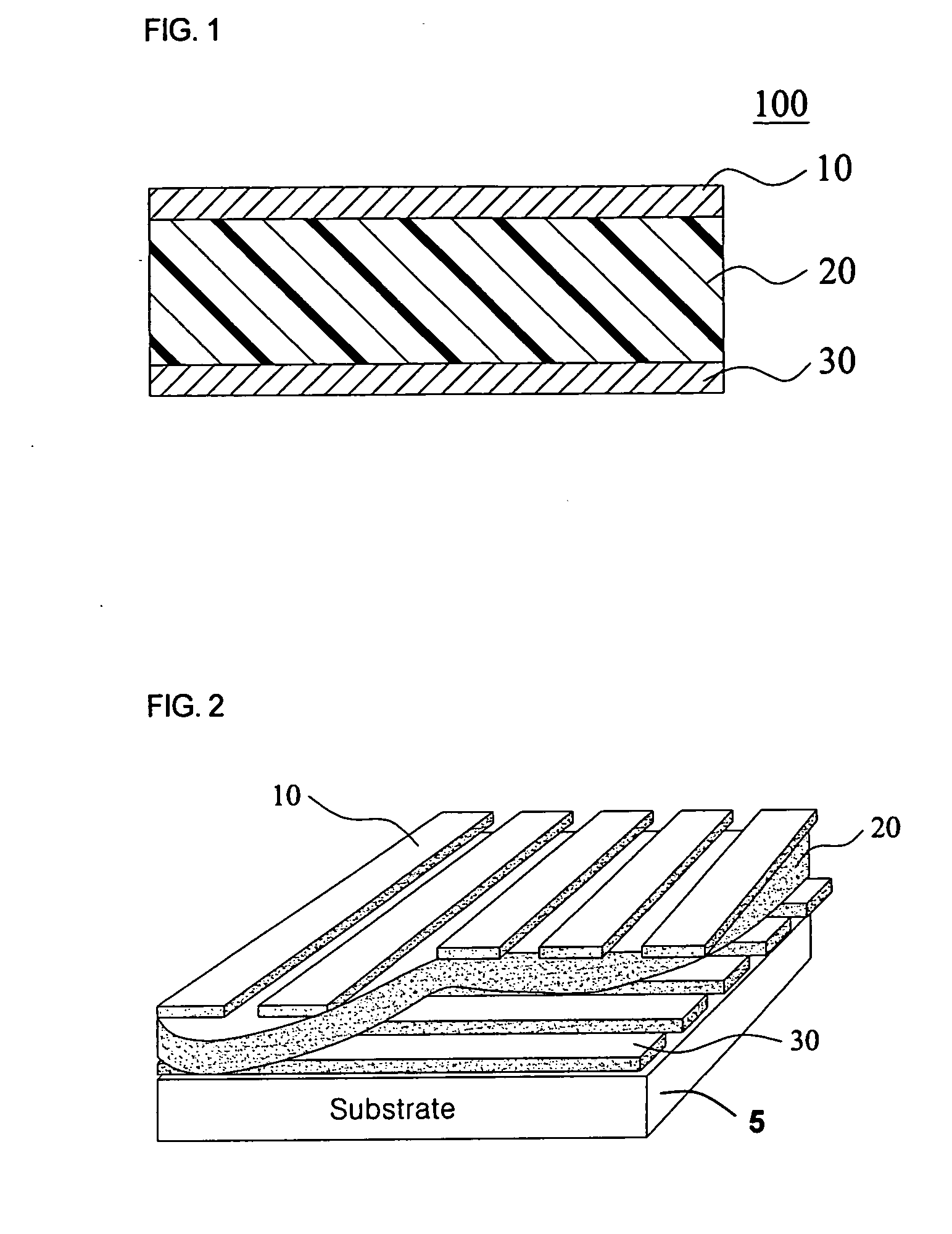
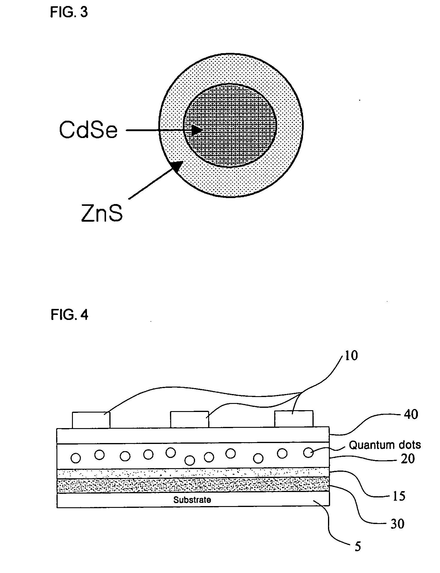
[0036] On a glass substrate having an aluminum (Al) lower electrode layer deposited thereon, a solution of CdSe (core) / ZnS (shell) quantum dots (1 wt %) obtained in the Preparative Example and poly(3-hexylthiophene) conductive polymer (9 wt %) in toluene was spin coated at 2500 rpm for 30 sec, and then baked at 60° C. for 30 min. Then, a barrier layer (Alq3) was deposited to a thickness of 20 nm on the coated substrate, and copper (Cu) was deposited on the barrier layer to form an upper electrode layer, thus obtaining a memory device. As such, the memory layer was 15 nm thick, and the electrode layers were 80 nm thick, in which the thickness of each layer was measured using an alpha-step profilometer. The electrode layer was deposited using a thermal evaporation process and the thickness of the electrode layer to be deposited was controlled using a quartz crystal monitor.

[0037] The current-voltage (I-V) curve of the above memory device is shown in FIG. 5, in which the voltage scan ...

example 2

[0038] On a glass substrate having an aluminum (Al) lower electrode layer deposited thereon, a solution of CdSe (core) / CdS / ZnS (shell) quantum dots (1 wt %) and poly(3-hexylthiophene) conductive polymer (9 wt %) in chloroform was spin coated at 25000 rpm for 30 sec, and then baked at 60° C. for 30 min. Then, a barrier layer (Alq3) was deposited to a thickness of 20 nm on the coated substrate, and copper (Cu) was deposited on the barrier layer to form an upper electrode layer, thus obtaining a memory device. As such, the memory layer was 20 nm thick, and the electrode layers were 80 nm thick, the thickness of each layer being measured using an alpha-step profilometer. The electrode layer was deposited using a thermal evaporation process and the thickness of the electrode layer to be deposited was controlled using a quartz crystal monitor.

[0039] The current-voltage (I-V) curve of the above device is shown in FIG. 6, in which the voltage scan is 0.1 volt / sweep. As shown in FIG. 6, a m...


PUM


Abstract

A memory device, which includes a memory layer having quantum dots uniformly dispersed in organic material disposed between an upper electrode layer and a lower electrode layer. The memory device is advantageous because it is nonvolatile and inexpensive, and realizes high integration and high speed switching. Further, size and distribution of the quantum dots may be uniform, thus realizing uniform memory behavior. Furthermore, the memory device is suitable for application to portable electronic devices that must have low power consumption, due to low operating voltages thereof.

Description

BACKGROUND OF THE INVENTION [0001] This non-provisional application claims priority under 35 U.S.C. §119(a) on Korean Patent Application No. 2004-111925 filed on Dec. 24, 2004, which is herein expressly incorporated by reference. [0002] 1. Field of the Invention [0003] Embodiments of the present invention relate, generally, to a memory device, and, more particularly, to a memory device including a memory layer having quantum dots uniformly dispersed in an organic material disposed between an upper electrode layer and a lower electrode layer, which is advantageous because it is nonvolatile and inexpensive, and realizes high integration, low power consumption, and high speed switching. [0004] 2. Description of the Related Art [0005] With the rapid development of the information and communication industries, the demand for various memory devices has drastically increased. In particular, memory devices used for portable terminals, various smart cards, electronic money, digital cameras, ...

Claims


Application Information

Patent Timeline
IPC IPC(8): H01L29/788
CPCB82Y10/00G11C13/0014H01L27/10G11C2216/08G11C13/0016Y10S977/783Y10S977/753
Inventor KANG, YOON SOKLEE, SANG KYUNJOO, WON JAE
Owner SAMSUNG ELECTRONICS CO LTD
Why Eureka
Try Eureka