

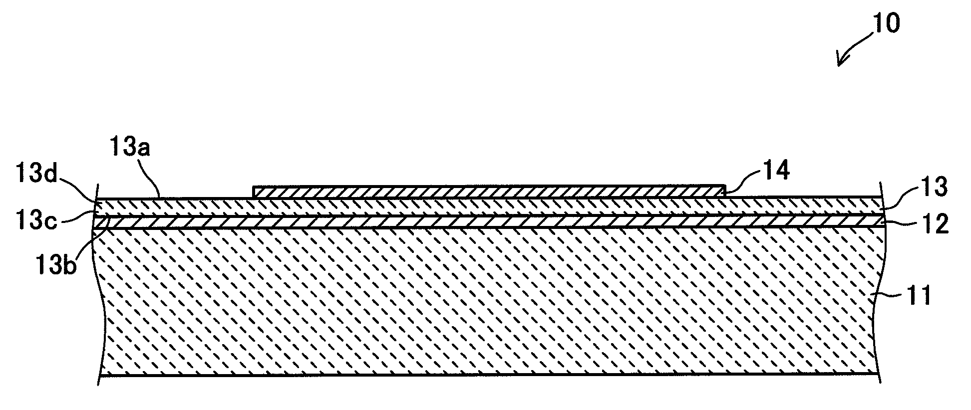
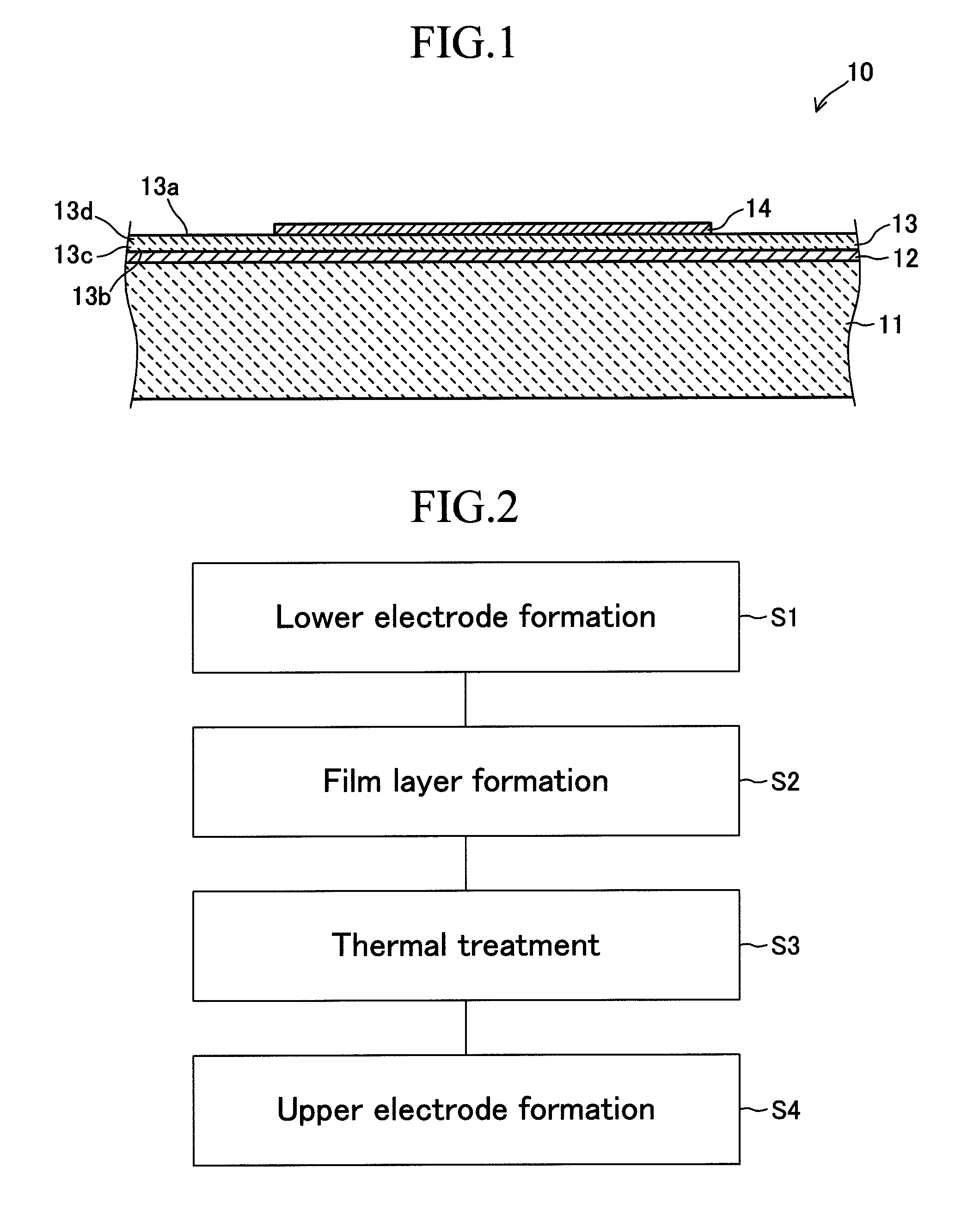
Dielectric device
a technology of dielectric devices and films, applied in the direction of electrode system manufacturing, device material selection, electric discharge tube/lamp manufacturing, etc., can solve the problems of fine metal particles not necessarily uniformly dispersed in the film layer, and fine metal particles may be non-uniformly dispersed, etc., to suppress impairment of properties, high efficiency, and high dielectric constant
- Summary
- Abstract
- Description
- Claims
- Application Information
AI Technical Summary
Benefits of technology
Problems solved by technology
Method used
Image

Examples
example 1
[0129]The electron emitter 120 of Example 1 (see FIG. 4) employs a zirconia substrate serving as a substrate 121. A lower electrode 122 is formed by coating the substrate 121 with a platinum paste through screen printing, followed by firing of the resultant coating film.
[0130]An emitter layer 123 is formed to have a thickness of 10 to 20 μm. The emitter layer 123 contains PZT (Zr:Ti=52:48) as the aforementioned dielectric material, and silver as the aforementioned metal.
[0131]An upper electrode 124 formed of flaky graphite powder is provided on the emitter layer 123. The upper electrode 124 is formed by coating the emitter layer 123 with a dispersion liquid prepared through dispersion of flaky graphite powder in a solvent containing an organic binder, followed by firing of the resultant coating film.
[0132]The aforementioned powdery dielectric material contained in raw material powder 81 (see FIG. 3) is PZT (Zr:Ti=52:48) having a number-based mean particle size of 1.0 μm. The aforeme...
example 2
[0147]The piezoelectric actuator 220 of Example 2 (see FIG. 11) employs a zirconia ceramic substrate serving as a substrate 221. A lower electrode 222 is formed by coating the substrate 221 with a platinum paste through screen printing, followed by firing of the resultant coating film.
[0148]A piezoelectric / electrostrictive layer 223 is formed to have a thickness of 10 to 20 μm. The piezoelectric / electrostrictive layer 223 contains PZT (Zr:Ti=52:48) as the aforementioned dielectric material, and silver as the aforementioned metal. The piezoelectric / electrostrictive layer 223 is formed under conditions similar to those employed in the case of Example 1.
[0149]An upper electrode 224 formed of gold thin film is provided on the piezoelectric / electrostrictive layer 223. The upper electrode 224 is formed by coating the piezoelectric / electrostrictive layer 223 with a gold paste through screen printing, followed by firing of the resultant coating film.
[0150]Table 2 shows the relation between ...
example 3
[0156]The electron emitter 120 of Example 3 (see FIG. 4) employs a soda glass substrate serving as a substrate 121. A lower electrode 122 and an upper electrode 124 are formed in a manner similar to that of Example 1.
[0157]An emitter layer 123 is formed to have a thickness of 10 to 20 μm. The emitter layer 123 contains PZT (Zr:Ti=52:48) as the aforementioned dielectric material, and silver as the aforementioned metal.
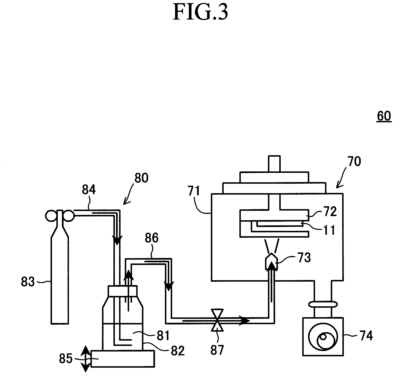
[0158]In the present Example, the emitter layer 123 is formed by means of an aerosol deposition apparatus 60 as shown in FIG. 14. The aerosol deposition apparatus 60 includes a deposition chamber 70. The deposition chamber 70 includes a nozzle 73 and an additional nozzle 73′ therein.
[0159]The aerosol deposition apparatus 60 includes an aerosol supply unit 80 and an additional aerosol supply unit 90. The aerosol supply unit 90 has the same configuration as the aerosol supply unit 80, and is configured such that an aerosol containing raw material powder 91 can be supplied...
PUM
| Property | Measurement | Unit |
|---|---|---|
| Fraction | aaaaa | aaaaa |
| Fraction | aaaaa | aaaaa |
| Fraction | aaaaa | aaaaa |
Abstract
Description
Claims
Application Information