Image display apparatus

a technology of image display and display device, which is applied in the direction of discharge tube/lamp details, discharge tube/lamp details, incadescent body mounting/support, etc., can solve the problems of degrading the reliability of the image display device, cracks may be formed in the panel glass sub, and the bonding material fgs on the surface of the gate electrode gl formed on the surface of the panel glass sub may be broken by the load, etc., to achieve excellent effect, high reliability, and high quality

Inactive Publication Date: 2007-09-27
HITACHI DISPLAYS
View PDF4 Cites 4 Cited by
  • Summary
  • Abstract
  • Description
  • Claims
  • Application Information

AI Technical Summary

Benefits of technology

[0031] According to the image display apparatus of the present invention, the partition includes a partition main body having curved portions at corners of upper and lower end portions contacting the cathode panel and anode panel and an electric conducting layer coated at least on the upper and lower end portions of the partition main body contacting the cathode panel and anode panel. Accordingly, the image display apparatus of high reliability and high quality can be realized and very excellent effects can be obtained, because only a small number of partitions are bonded and firmly fixed, without damaging the electrodes to be caused by the partitions mounted between the cathode panel and anode panel, and being independent from a coating precision and mount precision of the bonding material. The influence of charges on the partitions upon an electron trajectory can be eliminated, an insufficient luminance due to insufficient excitation of the fluorescent material layers can be prevented, so that an image display apparatus having high color reproduction can be realized and very excellent effects can be obtained.

Problems solved by technology

On the other hand, as shown in a main part enlarged cross sectional view of FIG. 21, there arises an issue that when the partition SPC is mounted on the panel glass SUB, the bonding material FGS on the gate electrode GL formed on the surface of the panel glass SUB may be broken by the load LD or a crack CRK may be formed in the panel glass SUB.
There arises therefore an issue of degraded reliability of the image display apparatus, because the crack CRK is likely to be formed in the panel glass SUB so that this crack may become a generation source of vacuum leakage, resulting in a low air-tight state and a deteriorated vacuum degree in the inner space (in the air-tight space) constituted of the panel glass SUB and sealing frame.
There arises an issue of degraded reliability of the image display apparatus to be caused by lowered conductivity and corresponding broken wiring due to damages of the gate electrode GL and the like.

Method used


Image

  • Image display apparatus
  • Image display apparatus
  • Image display apparatus

Examples


first embodiment

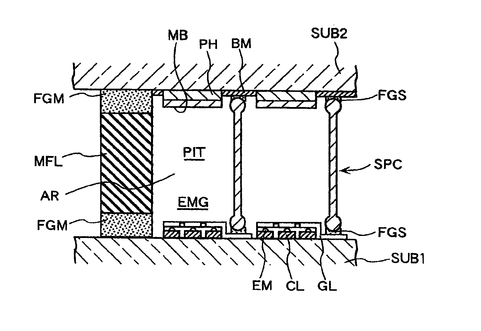
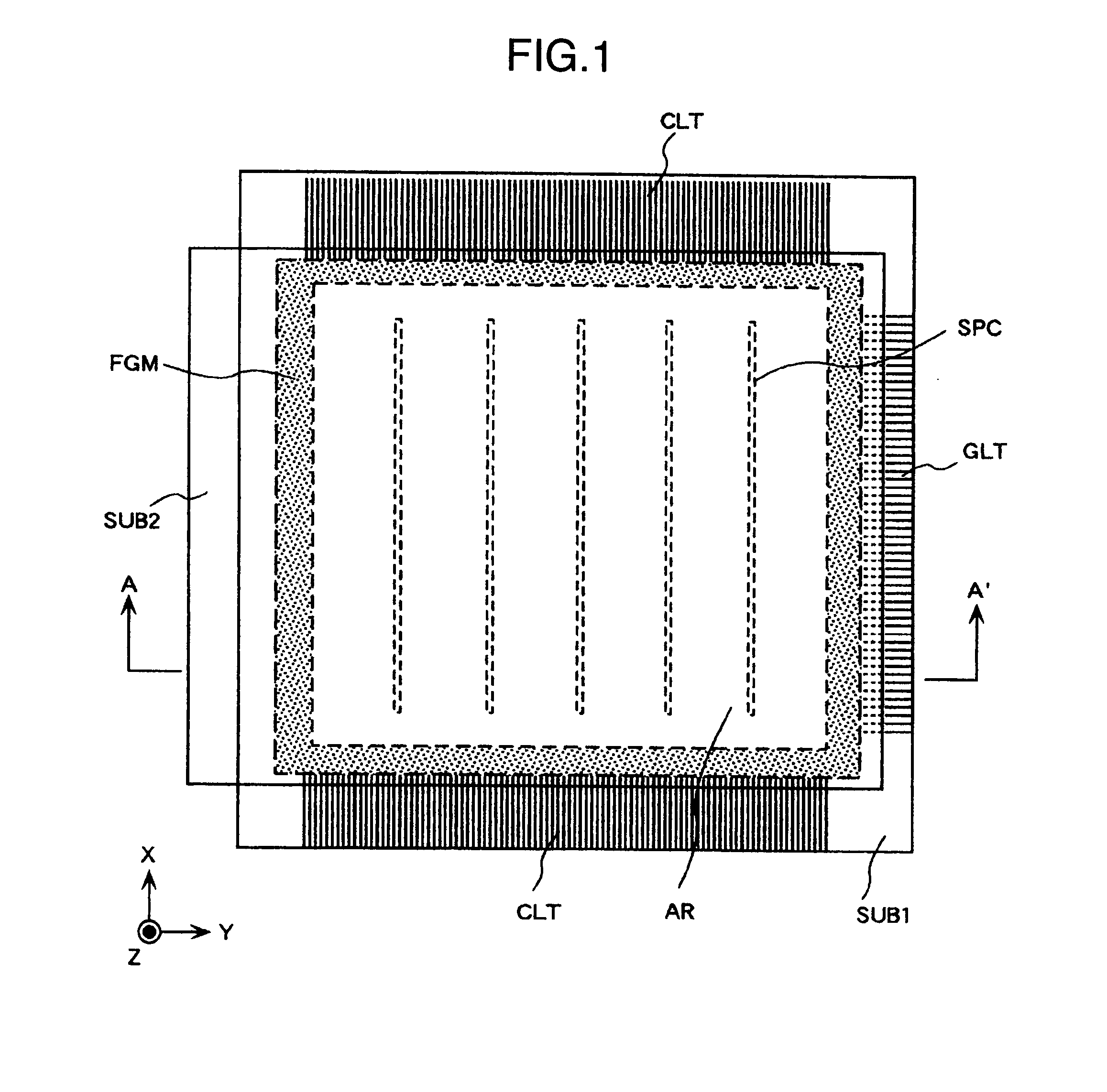
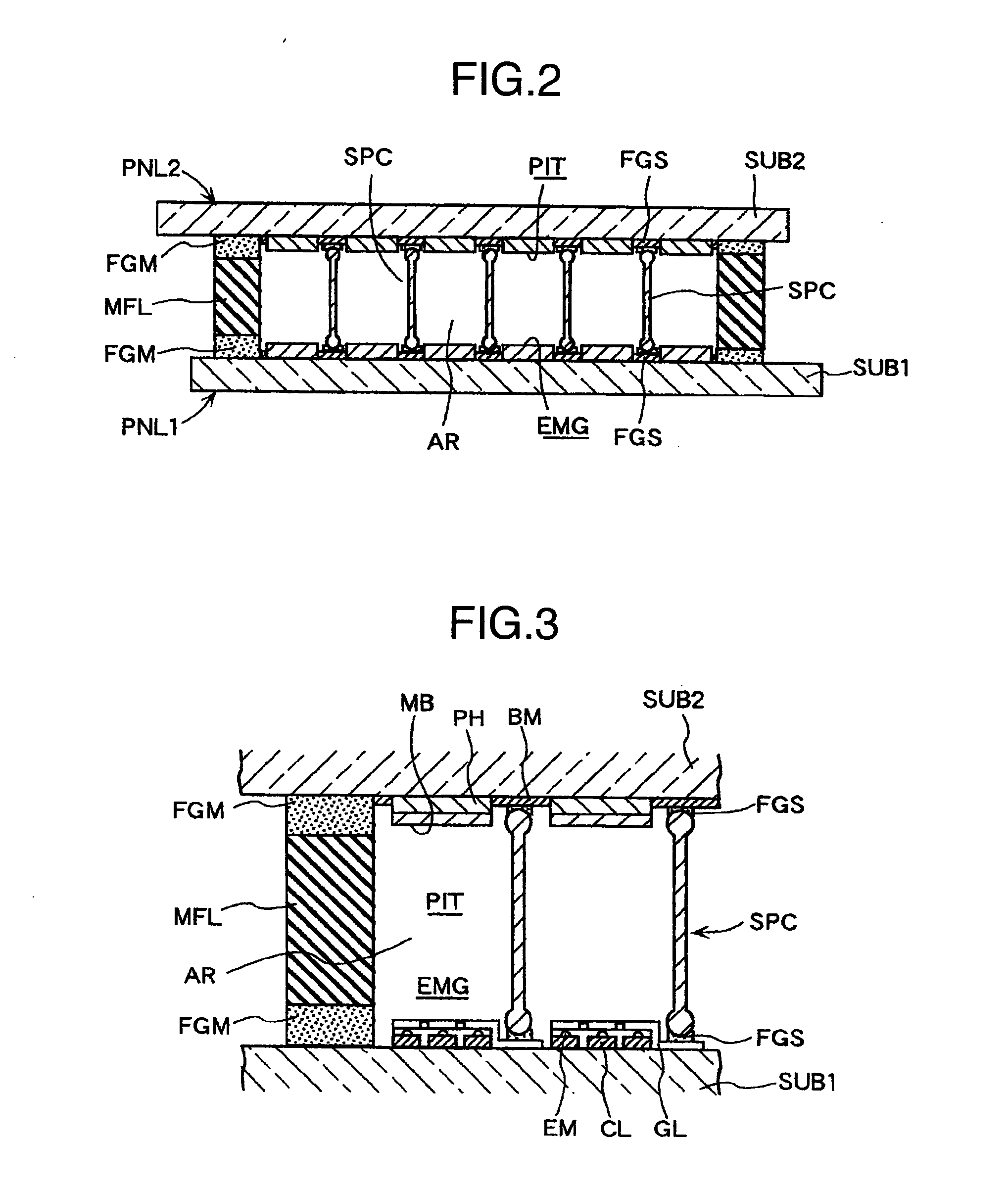
[0055] FIGS. 1 to 3 show an image display apparatus according to the first embodiment of the present invention. FIG. 1 is a schematic plan view showing the outline structure of the image display apparatus as viewed from an anode panel side, FIG. 2 is a schematic cross sectional view taken along line A-A′ shown in FIG. 1, and FIG. 3 is a main part enlarged cross sectional view of FIG. 2.

[0056] In these drawings, reference symbol SUB1 represents a back substrate constituting a cathode panel PNL1, SUB2 represents a front substrate constituting an anode panel PNL2, MFL represents a sealing frame, SPC represents a partition, EMG represents an electron emission element group, CL represents a cathode electrode, CLT represents a cathode electrode lead terminal, EM represents an electron source, GL represents a gate electrode, GLT represents a gate electrode lead terminal, PIT represents an image forming member, PH represents a fluorescent material layer, MB represents a metal back film (an...

second embodiment

[0069]FIGS. 6A and 6B are diagrams illustrating the structure of a partition SPC according to the second embodiment of the present invention. FIG. 6A is a main part perspective view and FIG. 6B is a cross sectional view. Like elements to those in the already described drawings are represented by identical reference symbols, and the description thereof is omitted. A different point of FIGS. 6A and 6B from FIGS. 4A and 4B resides in that the partition SPC has a vertically elongated ellipsoidal shape and the cross section of the partition main body NG has a width of a central portion wider than a width of upper and lower end portions as viewed in a cross section along a direction toward the back substrate and opposing front substrate.

[0070] Similar to the first embodiment, the partition main body NG is formed by molding glass material containing rare-earth elements by a redraw method using a glass reflow system. The partition main body NG is also coated with a silica film (not shown) ...

third embodiment

[0081]FIGS. 10A, 10B and 10C are perspective views illustrating the structure of partitions SPC according to the third embodiment of the present invention. Like elements to those in the already described drawings are represented by identical reference symbols, and the description thereof is omitted. A partition SPC shown in FIG. 10A has a partition main body NG made of a plate mold of glass material containing rare-earth elements, and each edge portion E has a curved plane having a diameter of curvature of about several μm to present the structure improving wettability (adhesion) to a bonding material (not shown). An electric conducting layer CO is coated on the outer peripheral surface of the partition SPC.

[0082] A partition SPC shown in FIG. 10B has a partition main body NG made of a plate mold of glass material containing rare-earth elements. The shape of the partition main body NG is a vertically elongated hexagonal shape and the cross section thereof has a width of a central p...


PUM

PropertyMeasurementUnit
flexural strengthaaaaaaaaaa
inclination angleaaaaaaaaaa
thicknessaaaaaaaaaa

Abstract

An image display apparatus is provided which is capable of suppressing generation of cracks to be caused by a load applied to a partition disposed between an anode panel and a cathode panel. The partition for retaining a predetermined distance between back and front substrates by using bonding material is constituted of a partition main body and an electric conducting layer coated on the outer peripheral surface of the partition main body. The partition main body has curved portions at the corners of upper and lower end portions, the curved portions contacting the back and front substrates. It is possible to prevent damages of an electrode to be caused by a mechanical load applied to cathode and anode panels having electrodes on opposing surfaces.

Description

CROSS-REFERENCE TO RELATED APPLICATION [0001] This application relates to an application U.S. Ser. No. being filed based on Japanese patent application No. 2004-372090 filed on Dec. 22, 2004, assigned to Hitachi Limited.BACKGROUND OF THE INVENTION [0002] 1. Field of the Invention [0003] The present invention relates to a luminescence type flat panel image display apparatus utilizing electron emission in vacuum, and more particularly to an image display apparatus having a display panel structured by disposing a plurality of partitions for holding a cathode panel and an anode panel at a predetermined space. The cathode panel has electron sources for emitting electrons by electric field emission, and the anode panel has an electron acceleration electrode and fluorescent material layers of plural colors which become luminous by excitation of electrons extracted from the cathode panel. [0004] 2. Description of the Related Art [0005] Color cathode ray tubes have been used conventionally a...

Claims


Application Information

Patent Timeline
Patent Type & Authority Applications(United States)
IPC IPC(8): H01J1/88H01J63/04H01J1/62
CPCC03C3/04C03C3/06C03C3/095H01J29/864H01J2329/866H01J2329/863H01J2329/864H01J2329/8645H01J31/127
Inventor SAWAI, YUICHISHIONO, OSAMUMIYATA, MOTOYUKIAKATA, HIROYUKIINOUE, YUICHINAITO, TAKASHIKANAZAWA, KEIICHIKOBAYASHI, KINYA
Owner HITACHI DISPLAYS
Why Eureka
Try Eureka