Laterally Implanted Electroabsorption Modulated Laser

a modulation laser and laser technology, applied in semiconductor lasers, instruments, non-linear optics, etc., can solve the problems of limited modulation efficiency, poor reliability and manufacturing complexity, and low output power, and achieve the effect of reducing the capacitance of the modulator

Inactive Publication Date: 2007-09-27
BOOKHAM TECH
View PDF12 Cites 16 Cited by
  • Summary
  • Abstract
  • Description
  • Claims
  • Application Information

AI Technical Summary

Benefits of technology

[0013] It is therefore an object of the present invention to provide an improved monolithically integrated electroabsorption modulated laser (EML). In particular, it is an object of the present invention to provide a monolithically integrated electroabsorption modulated laser wherein the modulator is of shallow etched ridge waveguide design by using ion implantation of the etched upper cladding layer to reduce capacitance of the modulator.

Problems solved by technology

A drawback to the BH laser format, however, can be lower output power, poor reliability and more complexity of manufacture when compared to a ridge wave guide (RWG) laser format.
This device has a disadvantage of the BH configuration as well as requiring many discrete process steps to produce the laser and the modulator separately.
Other possible disadvantages include limited modulation efficiency and less than ideal coupling between the laser and EAM, due to the hybrid growth technique.
Here, both the laser and EAM are of a BH configuration and can benefit from common process steps in manufacture but still have the disadvantages of the BH configuration.
A ridge waveguide (RWG) laser could provide output power benefits over deep etched and BH lasers, but the shallow etch required for a RWG laser would be incompatible with the deep etch required for traditional EAMs.
Disadvantages of this possible solution include increased. costs for the extra processing steps of separate etches for the laser and the EAM, a deep etch and burial-overgrowth for the laser, and stringent manufacturing tolerances required for the transition region.

Method used


Image

  • Laterally Implanted Electroabsorption Modulated Laser
  • Laterally Implanted Electroabsorption Modulated Laser
  • Laterally Implanted Electroabsorption Modulated Laser

Examples


Embodiment Construction

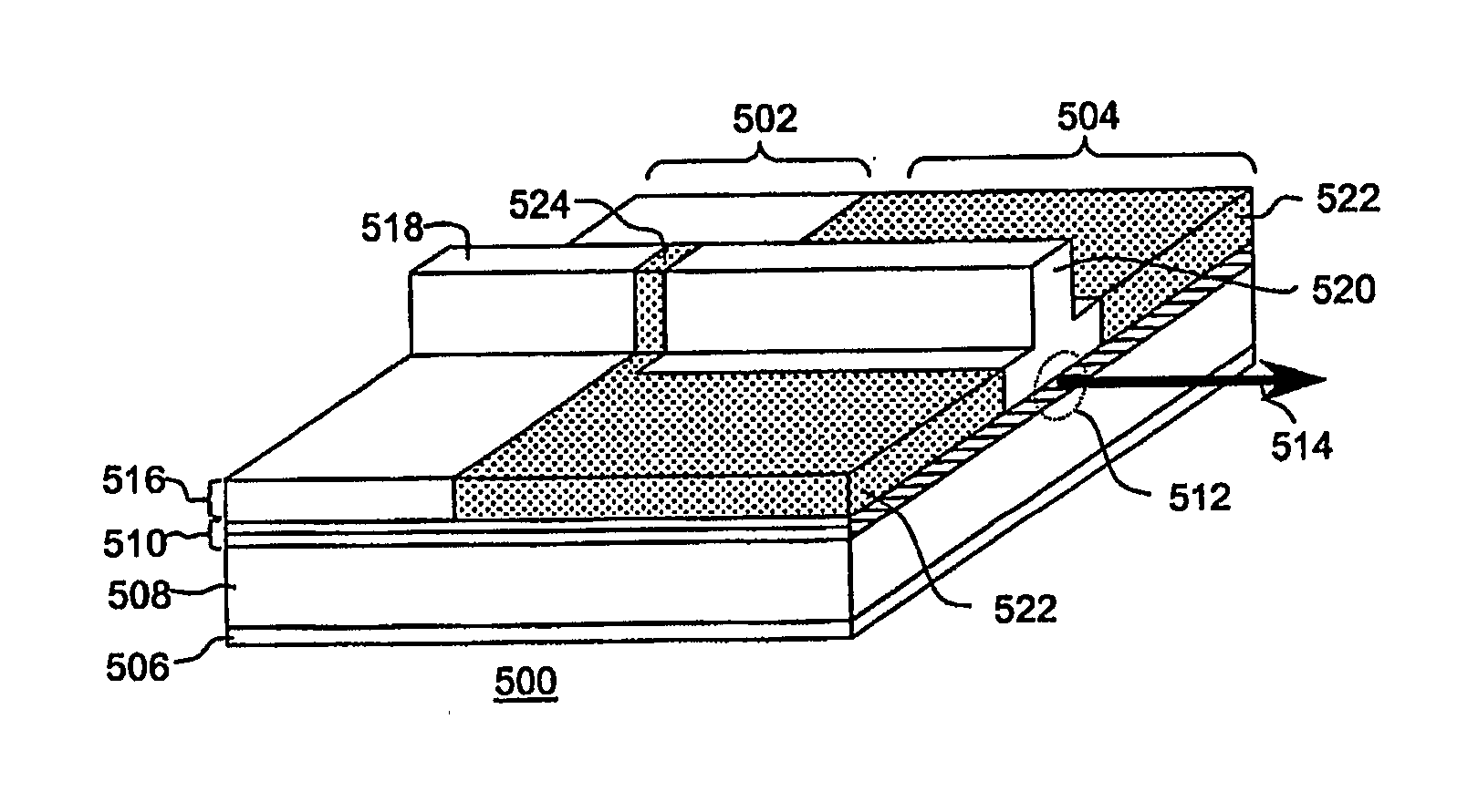
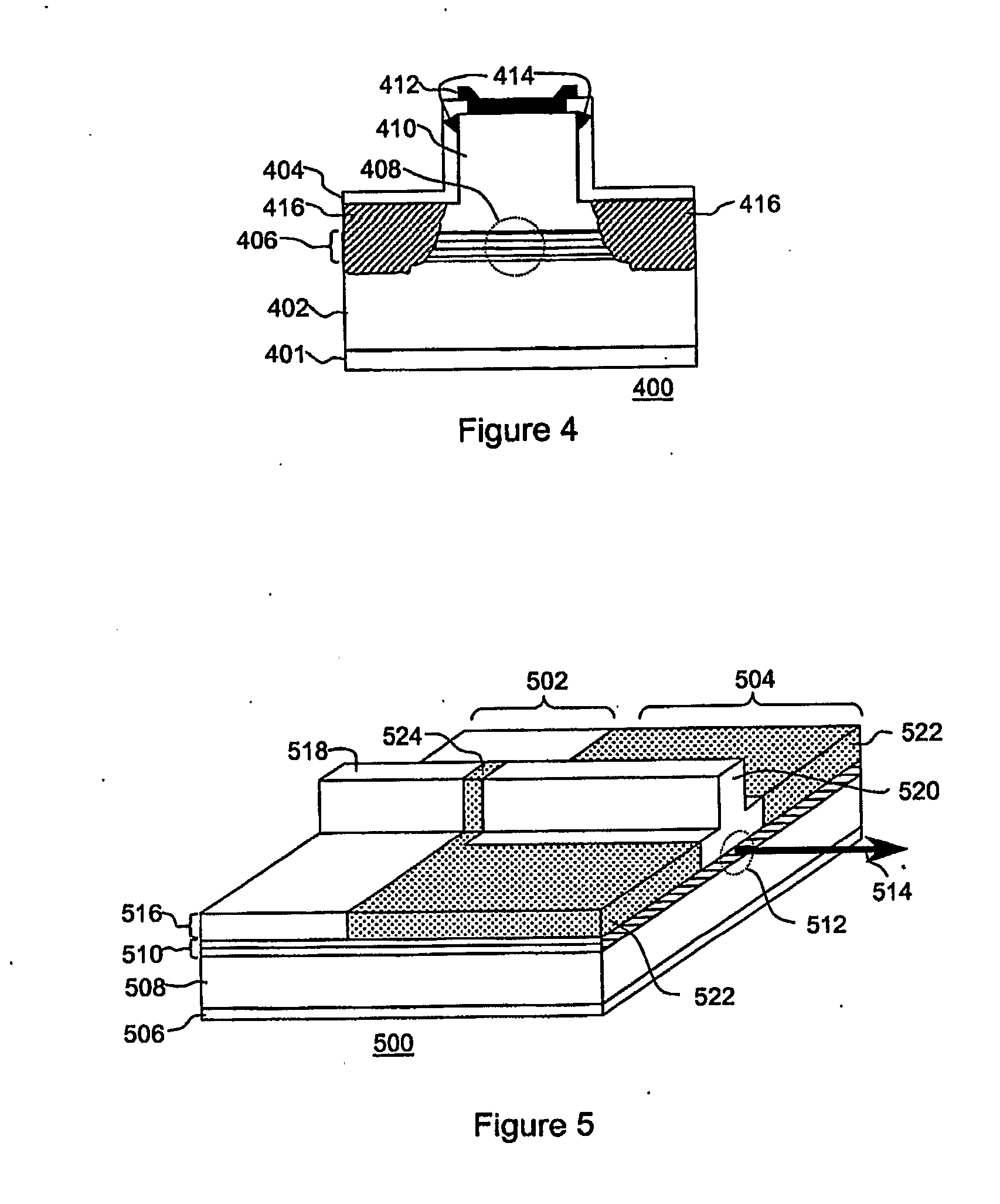
[0057] Generally, the present invention provides a monolithically integrated electroabsorption modulated laser wherein the modulator is of shallow etched ridge waveguide design which uses ion implantation of the etched upper cladding layer to reduce capacitance of the modulator.

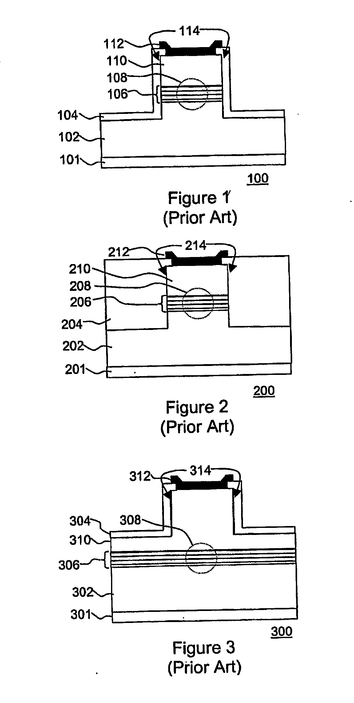
[0058]FIG. 1 is a simplified illustration of a prior art deeply etched optoelectronic device 100. FIG. 1 can represent a semiconductor laser or an electroabsorption modulator (EAM). A laser or an EAM are constructed of similar materials, but would differ in design details and operation. The device of FIG. 1 will now be described as an EAM 100. The EAM 100 is deeply etched. It comprises a semiconductor substrate 101, an active layer 106, followed by an upper cladding layer 110 and a metal electrode 112. The optical mode 108 is approximately centered around the active layer 106 which functions as a vertical waveguide. The horizontal waveguide function is provided by the deeply etched ridge of material bounded ...


PUM

PropertyMeasurementUnit
capacitanceaaaaaaaaaa
optical energyaaaaaaaaaa
epitaxial structureaaaaaaaaaa

Abstract

A monolithically integrated electroabsorption modulated laser having a ridge waveguide structure, has lateral ion implantation. The integrated device has a laser section and a modulator section. The modulator section has ion implanted regions adjacent to the waveguide ridge. The implanted regions penetrate through the top cladding layer to reduce capacitance within the intrinsic active core of the reverse biased modulator and allow a shallow etched ridge waveguide structure to be used for the modulator. The device provides good optical coupling, efficient manufacturing, and good high power performance.

Description

CROSS-REFERENCE TO RELATED APPLICATIONS [0001] This is the first application filed for the present invention. MICROFICHE APPENDIX [0002] Not Applicable. TECHNICAL FIELD [0003] The present invention relates to the field of photonics and the construction of lasers and electroabsorption modulators, and more particularly with the construction of a monolithically integrated electroabsorption modulated laser. BACKGROUND OF THE INVENTION [0004] Electroabsorption modulators (EAMs) provide a convenient and efficient way of modulating optical communications signals, especially those generated by laser sources. Combining a laser and an EAM into a monolithically integrated electroabsorption modulated laser (EML) can reduce manufacturing costs, assembly costs and footprint. An important consideration in monolithically integrating a laser and modulator on a single waveguide is that there must be good optical coupling between the two sections—there must be a good overlap between their optical mode...

Claims


Application Information

Patent Timeline
Patent Type & Authority Applications(United States)
IPC IPC(8): H01S5/026G02F1/015G02F1/017G02F1/21H01L21/265H01L27/00H01S5/022H04B10/17
CPCB82Y20/00G02F1/015G02F1/01708G02F1/025G02F2001/0157H01S5/22G02F2201/063G02F2202/108H01L21/265H01S5/0265H01S5/2063G02F2001/212G02F1/0157G02F1/212
Inventor PROSYK, KELVINHAYSOM, JOAN
Owner BOOKHAM TECH
Why Eureka
Try Eureka