Semiconductor device

a semiconductor device and semiconductor technology, applied in the direction of solid-state devices, electric vehicles, loop antennas, etc., can solve the problems of difficult to secure power for transmitting/receiving long-distance signals, and become inability to generate the power necessary for individual information transmission/reception, etc., to achieve the effect of powering the semiconductor device enough and extending the communication distance with the reader/writer

Inactive Publication Date: 2007-10-04
SEMICON ENERGY LAB CO LTD
View PDF12 Cites 117 Cited by
  • Summary
  • Abstract
  • Description
  • Claims
  • Application Information

AI Technical Summary

Benefits of technology

[0026]A semiconductor device of the present invention has a battery; therefore, it can be prevented that power for transmitting / receiving individual information gets low in accordance with deterioration over time of a battery. In addition, a semiconductor device of the present invention has an antenna for supplying power to a battery wirelessly. Therefore, the semiconductor device can charge the battery by utilizing power of an external electromagnetic wave as a power source for driving the semiconductor device without being directly connected to a charger. Thus, it becomes possible to continue to use the semiconductor device without a check of remaining capacity of a battery or a change of the battery, which is necessary in the case of an active RFID. In addition, power for driving the semiconductor device is always held in the battery, whereby power enough for operation of the semiconductor device can be obtained and communication distance with the reader / writer can be extended.

Problems solved by technology

However, there has been a problem in that a semiconductor device including an active RFID provided with a driving battery, which is shown in FIG. 31, consumes power over time in accordance with transmission / reception of individual information, and setting of intensity of a radio wave necessary for the transmission / reception, and finally, it becomes impossible to generate power necessary for the transmission / reception of individual information.
Therefore, there has been a problem in that it is required that remaining capacity of a driving battery be checked and the driving battery be changed in order to continue to use a semiconductor device including an active RFID which is provided with the driving battery.
Further, as shown in FIG. 32, a semiconductor device, which has a passive RFID that generates driving power by utilizing an external electromagnetic wave (carrier wave), has a problem in that it is difficult to secure power for transmitting / receiving a long-distance signal and for transmitting an electromagnetic wave necessary for the transmission / reception and to realize a good transmission / reception state.
Therefore, there has been a problem in that a semiconductor device, which has a passive RFID that generates driving power by utilizing an external electromagnetic wave (carrier wave), can be used only when an external electromagnetic wave is sufficiently supplied (for example, when the semiconductor device is provided near an antenna of a reader / writer which is a power source supplying means).

Method used


Image

  • Semiconductor device
  • Semiconductor device
  • Semiconductor device

Examples


embodiment mode 1

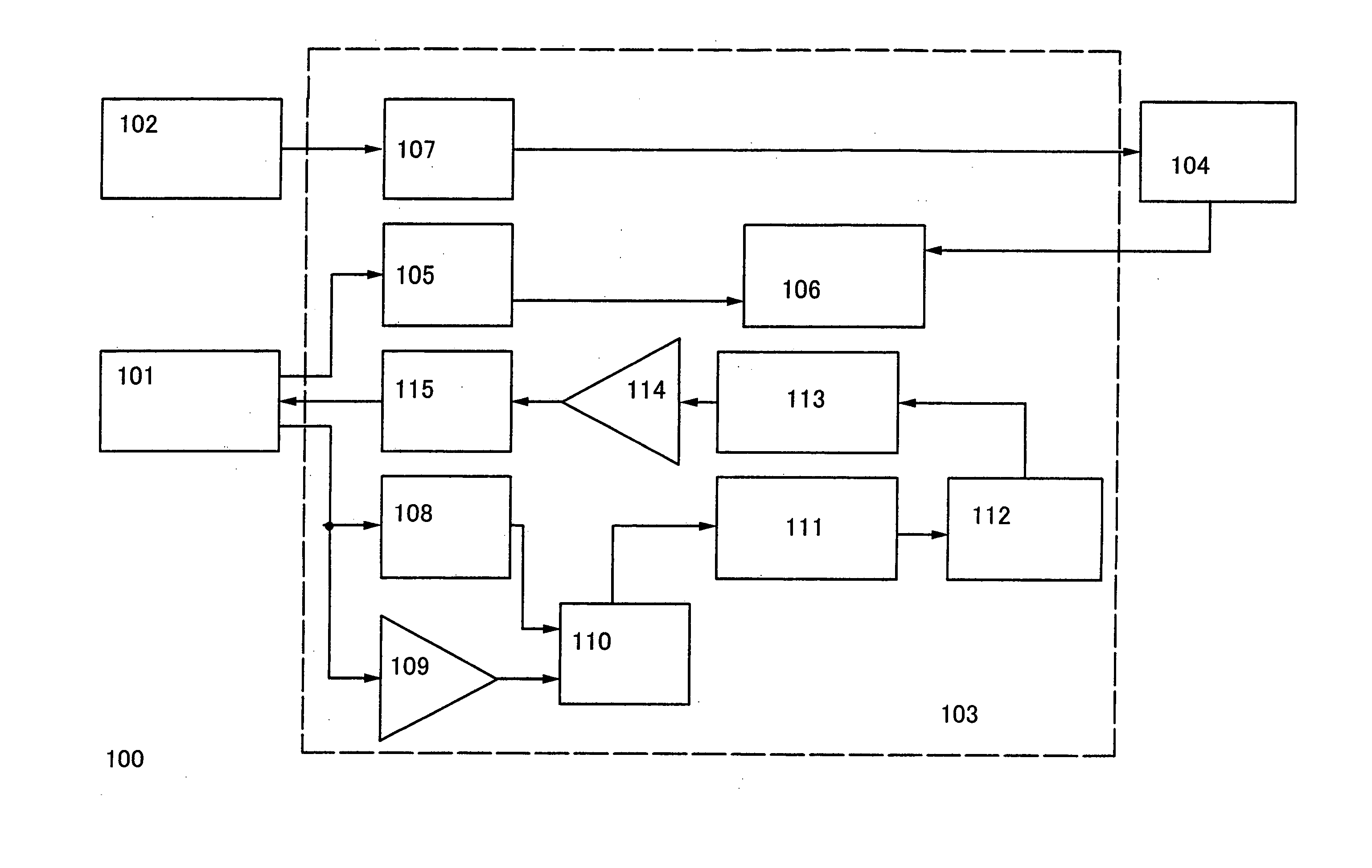
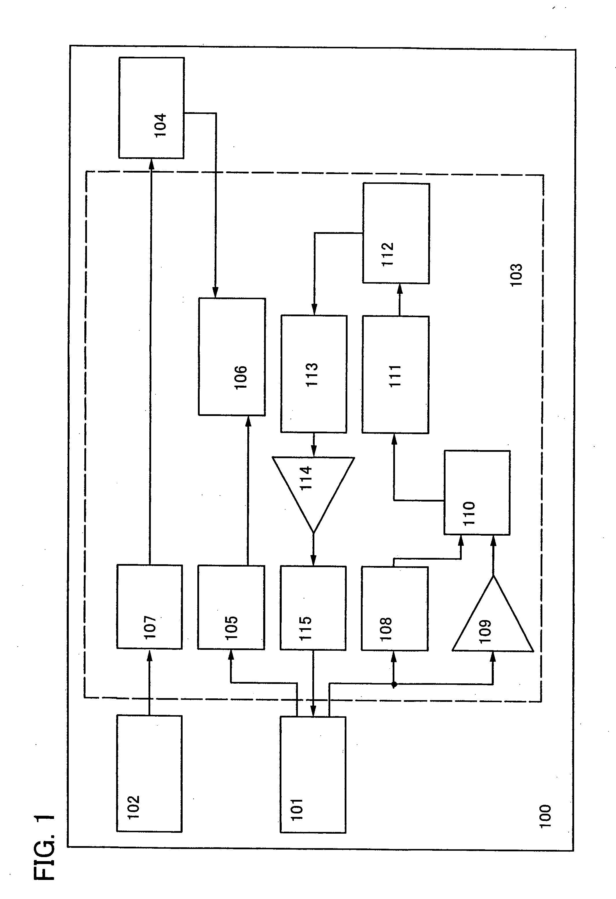
[0069]A structure example of a semiconductor device of the present invention is described with reference to block diagrams shown in FIGS. 1 and 2. Note that in this embodiment mode, description is made of a case where a semiconductor device is used as an RFID tag (hereinafter, also simply referred to as “RFID”).

[0070]A semiconductor device shown in FIG. 1 (hereinafter referred to as an “RFID 100”) includes a first antenna circuit 101, a second antenna circuit 102, a signal processing circuit 103, and a battery 104. The signal processing circuit 103 includes a first rectifier circuit 105, a power source circuit 106, a second rectifier circuit 107, a demodulation circuit 108, an amplifier 109, a logic circuit 110, a memory control circuit 111, a memory circuit 112, a logic circuit 113, an amplifier 114, and a modulation circuit 115.

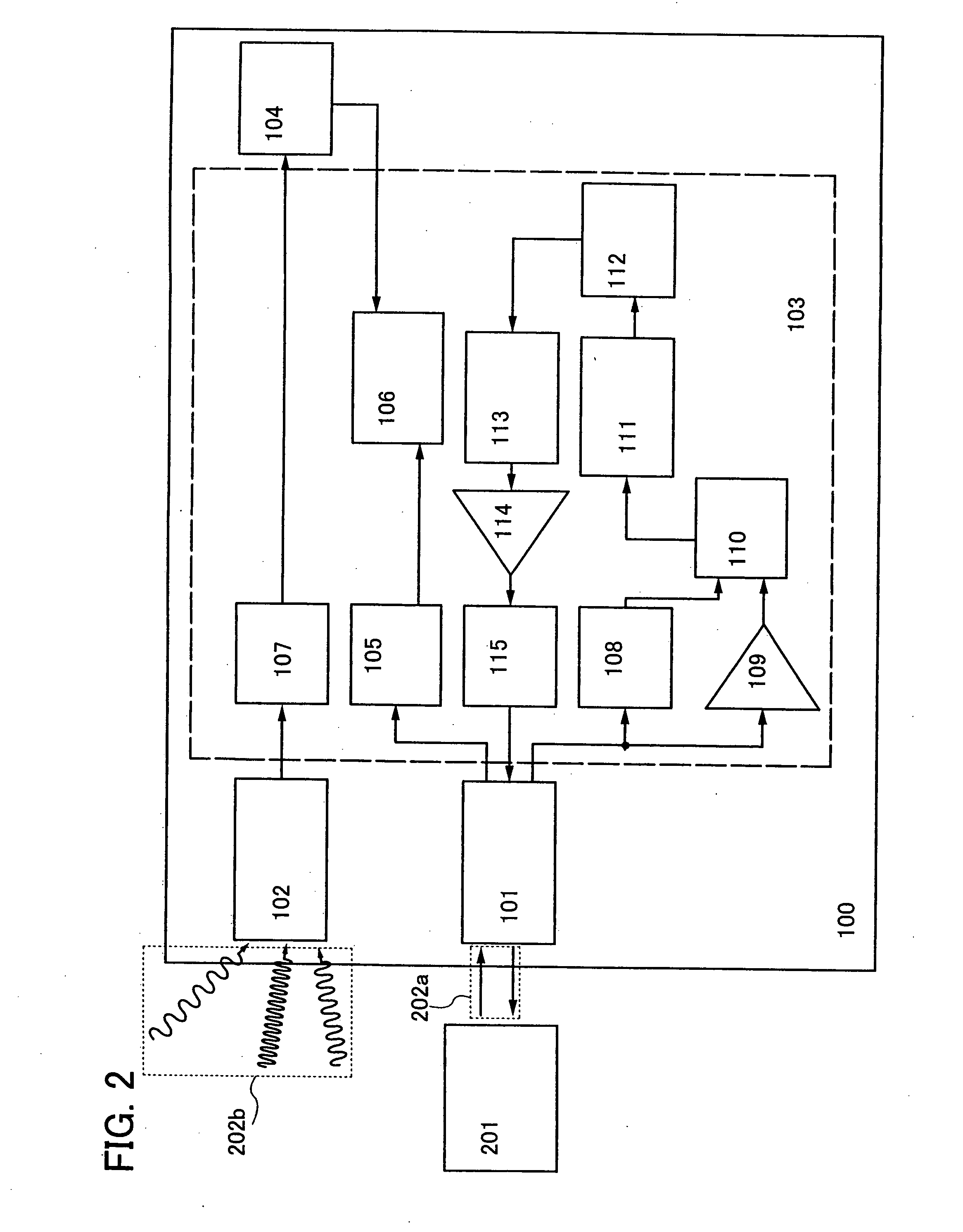
[0071]FIG. 2 shows a case where the first antenna circuit 101 receives a radio wave 202a generated from a reader / writer 201 (or transmits a radio wave to t...

embodiment mode 2

[0116]In this embodiment mode, description is made of a structure in which a booster antenna circuit (hereinafter referred to as a booster antenna) is provided in the semiconductor device including the RFID described in Embodiment Mode 1, with reference to drawings. Note that in drawings used in this embodiment mode, common portions to those in Embodiment Mode 1 are denoted by the same reference numerals in some cases.

[0117]A booster antenna described in this embodiment mode has a larger size than an antenna for receiving a signal from a reader / writer and outputting data to a signal processing circuit (hereinafter referred to as a first chip antenna or a first antenna circuit) and an antenna for receiving a radio signal to charge a battery (hereinafter referred to as a second chip antenna or a second antenna circuit) in a semiconductor device. A booster antenna can transmit / receive a signal to / from a reader / writer or receive a radio signal efficiently by being resonated in a frequen...

embodiment mode 3

[0139]In this embodiment mode, description is made of an example of a manufacturing method of the semiconductor device described in the aforementioned embodiment mode with reference to drawings.

[0140]First, as shown in FIG. 19A, a peeling layer 1903 is formed over one side of the substrate 1901 with an insulating film 1902 interposed therebetween. Subsequently, an insulating film 1904 that function as base film and a semiconductor film 1905 (for example, a film containing amorphous silicon) are stacked. Note that the insulating film 1902, the peeling layer 1903, the insulating film 1904, and the semiconductor film 1905 can be sequentially formed.

[0141]As the substrate 1901, a glass substrate, a quartz substrate, a metal substrate (such as a ceramic substrate or a stainless steel substrate), or a semiconductor substrate such as a Si substrate can be used. Alternatively, a substrate formed of polyethylene terephthalate (PET), polyethylene naphthalate (PNT), polyether sulfone (PES), ac...


PUM


Abstract

An object is to provide a semiconductor device including an RFID which can transmit/receive individual information without a change of a battery accompanied by deterioration over time of the battery as a drive power source, and to which driving power can be supplied to keep a favorable transmission/reception state of the individual information even when an external electromagnetic wave is not sufficient. The semiconductor device includes a signal processing circuit, a first antenna circuit and a second antenna circuit operationally connected to the signal processing circuit, and a battery operationally connected to the signal processing circuit, in which the first antenna circuit transmits/receives a signal for transmitting data stored in the signal processing circuit; the second antenna circuit receives a signal for charging the battery; and a signal received by the first antenna circuit and a signal received by the second antenna circuit have different wavelengths.

Description

TECHNICAL FIELD[0001]The present invention relates to a semiconductor device. In particular, the present invention relates to a semiconductor device that transmits / receives data and receives power through a radio wave.BACKGROUND ART[0002]In recent years, an individual identification technology using wireless communication has attracted attention. In particular, as a semiconductor device which communicates data by wireless communication, an individual identification technology using an RFID (Radio Frequency Identification) tag has attracted attention. The RFID tag is also called an IC (Integrated Circuit) tag, an IC chip, an RF tag, a wireless tag, or an electronic tag. The individual identification technology using an RFID has started to help production, management, or the like of an individual object, and is anticipated to be applied to personal authentication.[0003]RFIDs can be categorized into two types: an active RFID capable of transmitting an electromagnetic wave containing in...

Claims


Application Information

Patent Timeline
Patent Type & Authority Applications(United States)
IPC IPC(8): G08B13/14H04Q5/22G06K19/06G06K19/07H02J7/00
CPCG06K19/06037G06K19/0707H01L2924/0002H01L23/5227H01L27/1214H01L27/1266H01L2223/6677H01M10/052H01M10/30H01M10/345H01M10/44H01Q1/2225H01Q1/248H01Q7/00H01Q9/285H01L2924/00H01L27/1255Y02E60/10
Inventor SHIONOIRI, YUTAKAKOYAMA, JUNKUROKAWA, YOSHIYUKIYAMAZAKI, SHUNPEIIKEDA, TAKAYUKIOSADA, TAKESHIATSUMI, TOMOAKIISHII, MASATO
Owner SEMICON ENERGY LAB CO LTD
Why Eureka
Try Eureka