Power supply structure for high power circuit packages

a power supply structure and high-power circuit technology, applied in the direction of printed circuit manufacturing, printed circuit aspects, semiconductor/solid-state device details, etc., can solve the problems of new validation and qualification expenses, limited pths and rfps, and technological gaps, so as to reduce resistance and inductance parasitic effects

Inactive Publication Date: 2007-10-04
IBM CORP
View PDF9 Cites 21 Cited by
  • Summary
  • Abstract
  • Description
  • Claims
  • Application Information

AI Technical Summary

Benefits of technology

[0013] It is still a further object of the invention to provide a power supply architecture for high power circuit package reducing the package su

Problems solved by technology

Multiplying the number of PTHs or RFPs allows increasing the power supplied to the electronic device however, the number of PTHs and RFPs is limited by the pitch of the PTHs and RFPs i.e., the maximum number of PTHs and RFPs that can be done per length unit according to the manufacturing process.
While new technologies like laser drilling are being developed, their bigger challenge is still the need to create holes into composite materials, cladded with metal foils, posing great challenges in the laser power management, especially when dealing with so many different materials and their properties.
Any change drives new validations and qualification expenses.
Currently there is a technological gap between the capability of generating a great number of holes into the core, and the continuous trend in silicon interconnections de

Method used


Image

  • Power supply structure for high power circuit packages
  • Power supply structure for high power circuit packages
  • Power supply structure for high power circuit packages

Examples


first embodiment

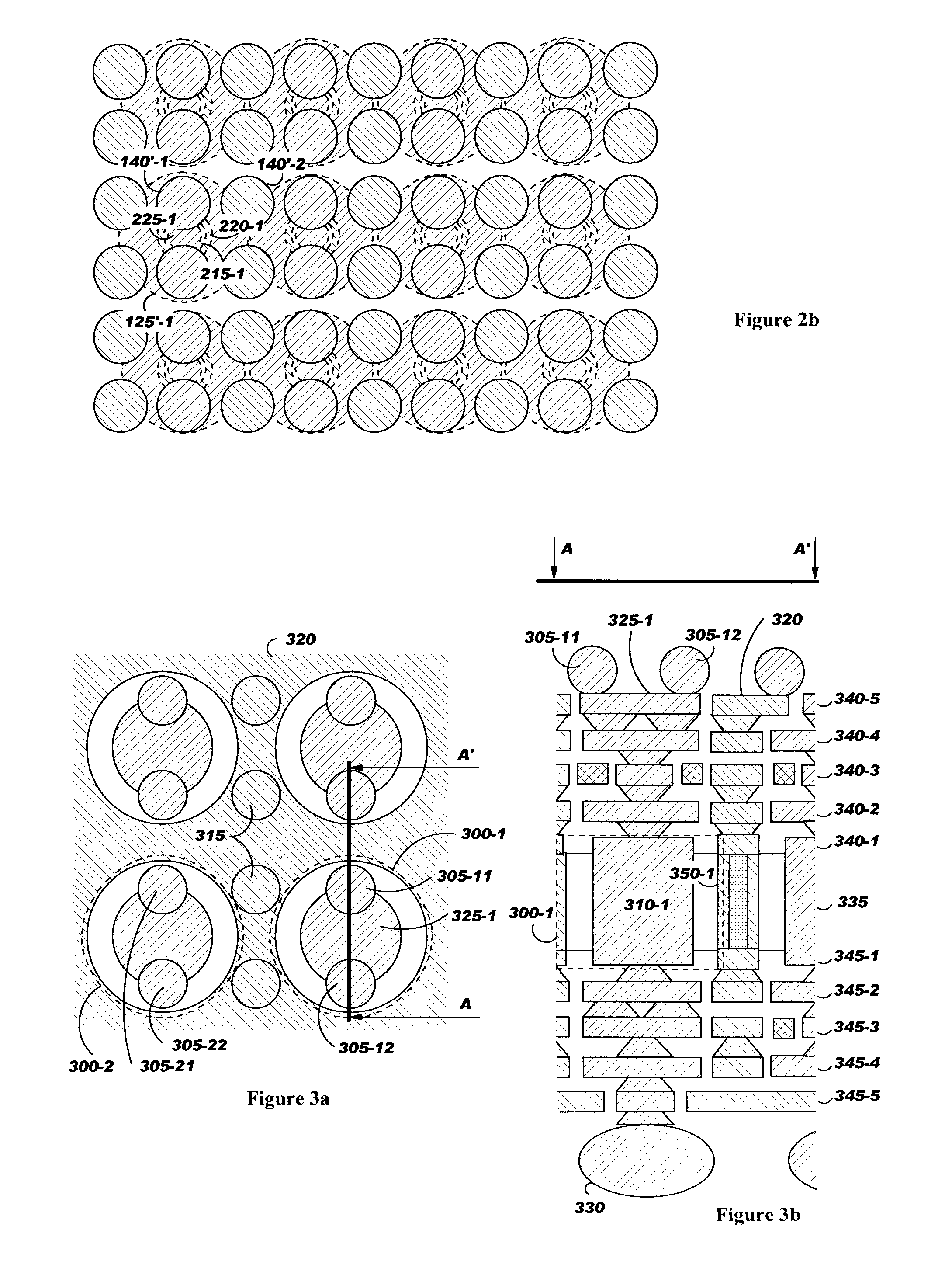
[0035]FIG. 3 illustrates a first embodiment wherein two C4 bumps are positioned at the periphery of the cylinder formed by each central conductive path of the coaxial structures, these two C4 bumps being connected to this central conductive path of the coaxial structure. FIG. 3a represents a top view of the electronic device carrier and FIG. 3b depicts a partial section view of the electronic device carrier along A-A′ axis. As shown, the two C4 bumps 305-11 and 305-12 are positioned at the periphery of the cylinder formed by the central part 310-1 of the coaxial structure 300-1. Likewise, the two C4 bumps 305-21 and 305-22 are positioned at the periphery of the cylinder formed by the central part of the coaxial structure 300-2. As depicted with hatching, the C4 bumps 305 are connected to the central part 310 of the coaxial structures 300 and so, share the same current level e.g., VDD. The C4 bumps 315 belonging to the columns positioned between the columns of C4 bumps 305 connected ...

second embodiment

[0037]FIG. 4 illustrates a second embodiment where one C4 bump is aligned on each central part of the coaxial structure. Similarly to FIG. 3, FIG. 4 comprises FIG. 4a that represents a top view of the electronic device carrier and FIGS. 4b and 4c that depict partial section views of the same electronic device carrier along B-B′ and C-C′ axis.

[0038] As shown, one C4 bump is aligned on the axis of each coaxial structure and one C4 bump is positioned approximately in the middle of two C4 bumps aligned on the axis of two adjacent coaxial structures. For example, C4 bump 405-22 is aligned on the axis of the coaxial structure 400-1, C4 bump 405-42 is aligned on the axis of the coaxial structure 400-2, and C4 bumps 405-32 and 415-22 are positioned between C4 bumps 405-22 and 405-42, and C4 bumps 405-22 and 405-23, respectively. The C4 bumps aligned on the axis of the coaxial structure are connected to the central part 410 of the coaxial structure, preferably according to a vertical path as...


PUM


Abstract

A power supply structure for high power circuit package is disclosed. According to the invention, the electrical connections between power planes are done through a plurality of coaxial structures that can be totally or partially implemented in the circuit shadow area of the electronic device carrier, for example under the engine area of the circuit. According to this principle, a same hole is used to transfer two different current levels, one on its periphery and the other one on its centre, doubling the electrical transfer capacity.

Description

FIELD OF THE INVENTION [0001] The present invention relates generally to the structure and manufacture of electronic printed circuit boards and chip carriers and more specifically to a particular power supply structure for high power circuit packages. BACKGROUND OF THE INVENTION [0002] An electronic device carrier comprises a thin plate formed of multiple layers onto which chips and other electronic components, such as capacitors, are mounted. Usually the half of layers of an electronic device carrier is dedicated to supply voltages planes. These supply voltages are supposed to be constant across the carrier and the chip, and are expected to operate reliably over the system's lifetime. [0003] With the advent of ultra-deep submicron technology and the contemporaneous growth of modem system, the current flow across the electronic device carrier is increasing and so, it is generally required to use multiple current paths for providing the electronic device with required current from th...

Claims


Application Information

Patent Timeline
IPC IPC(8): H05K1/11H05K1/14
CPCH01L23/49827H01L23/50H01L2924/0002H01L2223/6616H01L2223/6622H05K1/0222H05K1/112H05K1/115H05K3/4602H05K2201/09309H05K2201/09536H05K2201/096H05K2201/09809H01L2924/00
Inventor CASTRIOTTA, MICHELEOGGIONI, STEFANOSSPREAFICO, MAUROVIERO, GIORGIO
Owner IBM CORP
Why Eureka
Try Eureka