Semiconductor Device

a semiconductor device and memory circuit technology, applied in semiconductor devices, digital storage, instruments, etc., can solve the problems of reducing the inability to additionally write data, and achieve the effect of preventing false rewriting, high reliability of the semiconductor device, and increasing the drive voltag

Inactive Publication Date: 2007-10-04
SEMICON ENERGY LAB CO LTD
View PDF54 Cites 48 Cited by
  • Summary
  • Abstract
  • Description
  • Claims
  • Application Information

AI Technical Summary

Benefits of technology

[0030] According to the invention, a semiconductor device in which data can be written (written once, read many) other than during manufacturing of a chip and falsification by rewriting can be prevented. Further, a layer can be formed thickly without increase in drive voltage in rewriting or reading of data by adding a layer in ...

Problems solved by technology

A mask ROM has a simple structure, however, data is required to be written during the manufacturing steps, and thus data cannot be additionally written.
When a thin organic compound layer is...

Method used


Image

  • Semiconductor Device
  • Semiconductor Device
  • Semiconductor Device

Examples


embodiment mode 1

[0053] In this embodiment mode, a structure of a semiconductor device, particularly, an example of a structure in which a layer containing an organic compound provided between a pair of conductive layers (hereinafter also referred to as an organic compound layer) (the part having the above structure is hereinafter also referred to as an “organic memory element”)

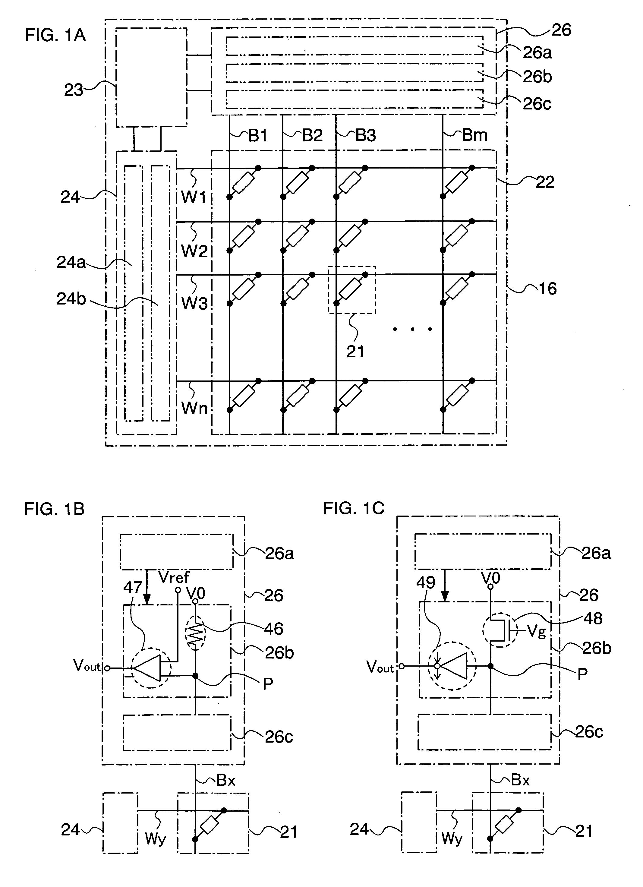
[0054]FIG. 1A shows an example of a structure of a memory circuit including an organic compound layer (hereinafter referred to as an organic memory). The memory circuit includes a memory cell array 22 in which memory cells 21 each including an organic memory element are arranged in matrix; a bit line driver circuit 26 including a column decoder 26a, a read circuit 26b, and a selector 26c; a word line driver circuit 24 including a row decoder 24a and a level shifter 24b; and an interface 23 having a writing circuit, which communicates with outside. Note that the structure shown here is only an example; accordingly, the memory...

embodiment mode 2

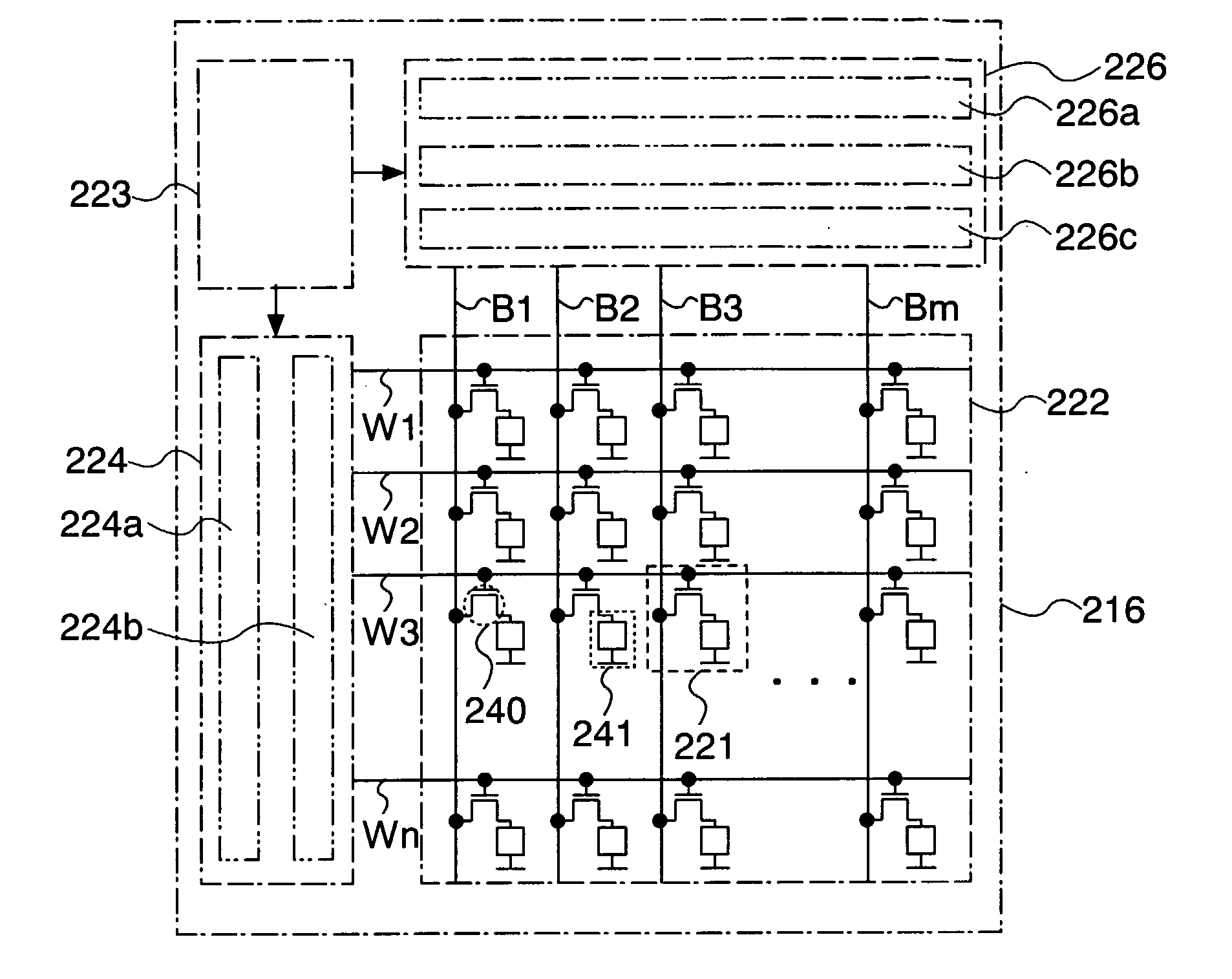
[0096] In this embodiment mode, a semiconductor device having a structure different from Embodiment Mode 1 will be described. Specifically, the case where the memory circuit has an active matrix structure will be shown.

[0097]FIG. 4A shows an example of a structure of an organic memory of this embodiment mode. The memory circuit includes a memory cell array 222 in which memory cells 221 are arranged in matrix; a bit line driver circuit 226 including a column decoder 226a, a read circuit 226b, and a selector 226c; a word line driver circuit 224 including a row decoder 224a and a level shifter 224b; and an interface 223 having a writing circuit, which communicates with outside. Note that the structure shown here is only an example; accordingly, the memory circuit 216 may include another circuit such as a sense amplifier, an output circuit, and a buffer, and the writing circuit may be provided on the bit line driver circuit.

[0098] The memory cell 221 includes a first wiring constituti...

embodiment mode 3

[0134] In this embodiment mode, another example of a semiconductor device different from the above embodiment mode will be explained with reference to drawings.

[0135] A semiconductor device shown in this embodiment mode is capable of non-contact reading and writing of data. Data transmission method is broadly classified into three of an electromagnetic coupling method of communicating by mutual induction with a pair of coils disposed in the opposed position, an electromagnetic induction method of communicating by an inductive electromagnetic field, and an electric wave method of communicating by using electric waves, and any of these methods may be employed. An antenna that is used for transmitting data can be provided in two ways. One way is to provide the antenna over a substrate provided with a plurality of elements, organic memory elements, and the like, and the other way is to provide a terminal portion on a substrate provided with a plurality of elements, organic memory eleme...


PUM


Abstract

It is an object of the present invention to provide a volatile organic memory in which data can be written other than during manufacturing and falsification by rewriting can be prevented, and to provide a semiconductor device including such an organic memory. It is a feature of the invention that a semiconductor device includes a plurality of bit lines extending in a first direction; a plurality of word lines extending in a second direction different from the first direction; a memory cell array including a plurality of memory cells each provided at one of intersections of the bit lines and the word lines; and memory elements provided in the memory cells, wherein the memory elements include bit lines, an organic compound layer, and the word lines, and the organic compound layer includes a layer in which an inorganic compound and an organic compound are mixed.

Description

TECHNICAL FIELD [0001] The present invention relates to a memory circuit including an organic compound and a semiconductor device including such a memory circuit. BACKGROUND ART [0002] In recent years, individual recognition technology has attracted attention. For example, there is a technology to be used for production and management, in which information such as a history of the object is clarified by giving an ID (an individual recognition code) to an individual object. Above all, the developments of semiconductor devices that can send and receive data without contact have been advanced. As such semiconductor devices, in particular, a wireless chip (also referred to as an ID tag, an IC tag, and IC chip, an RF (Radio Frequency) tag, a wireless tag, an electronic tag, or an RFID (Radio Frequency Identification)) is beginning to be introduced into companies, markets, and the like. [0003] Many of semiconductor devices that have already been put to practical use each have a circuit us...

Claims


Application Information

Patent Timeline
IPC IPC(8): G11C13/00
CPCB82Y10/00G11C13/0014G11C13/04H01L27/12H01L27/1266H01L27/13H01L27/1285H01L27/1292H10K19/10H10K85/631H01L21/82
Inventor ABE, HIROKOYUKAWA, MIKIOTAKANO, TAMAEASAMI, YOSHINOBUKOTO, KIYOSHINOMURA, RYOJIMARIYA, YOSHITAKA
Owner SEMICON ENERGY LAB CO LTD
Why Eureka
Try Eureka