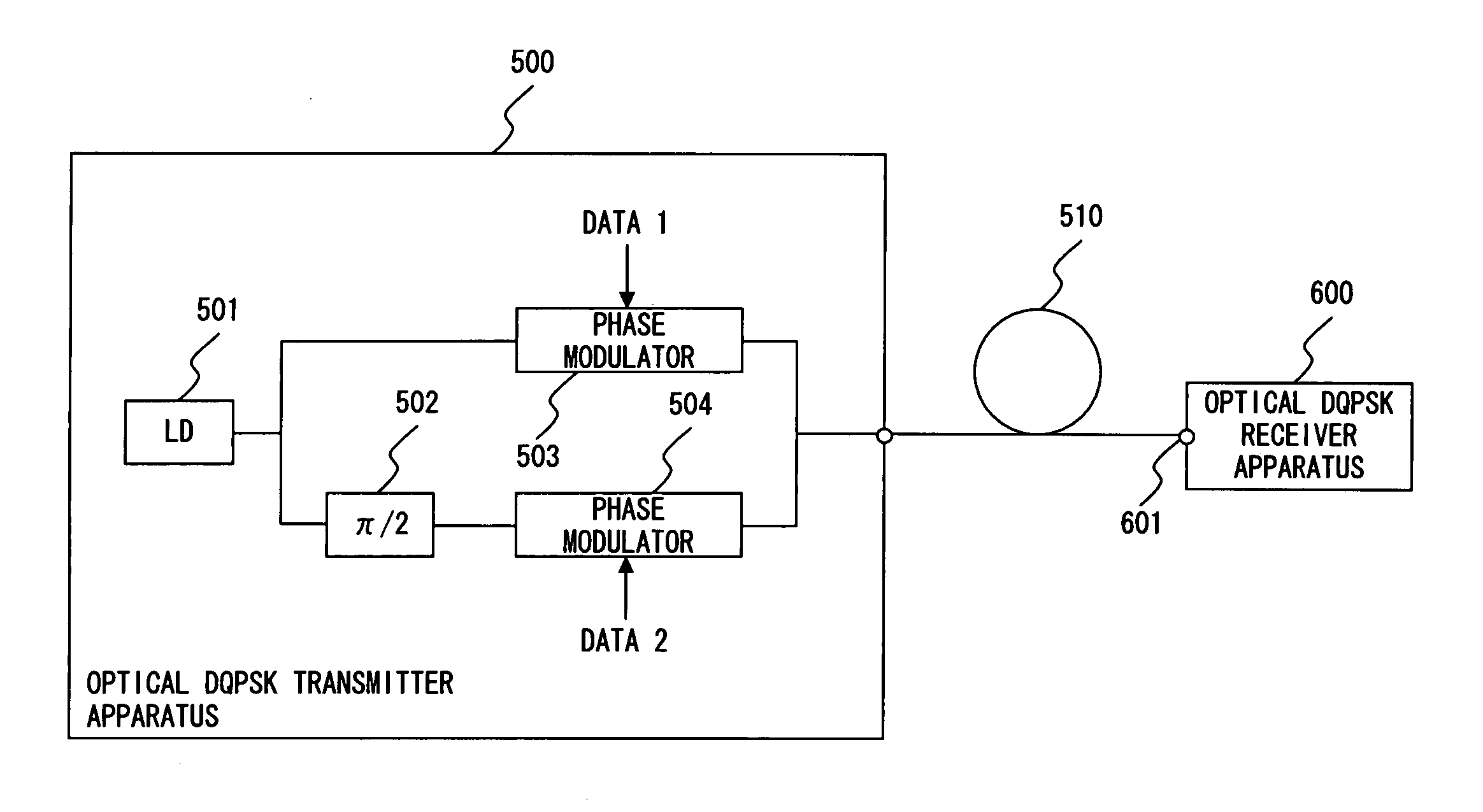
Optical DQPSK receiver apparatus
a receiver and optical technology, applied in the field of optical receivers, can solve the problems of complicated control of phase shift amount and high cost of high-speed photodiodes in general, and achieve the effect of reducing the number of interferometers that make up reducing the size and cost of the optical dqpsk receiver apparatus
- Summary
- Abstract
- Description
- Claims
- Application Information
AI Technical Summary
Benefits of technology
Problems solved by technology
Method used
Image

Examples
first embodiment
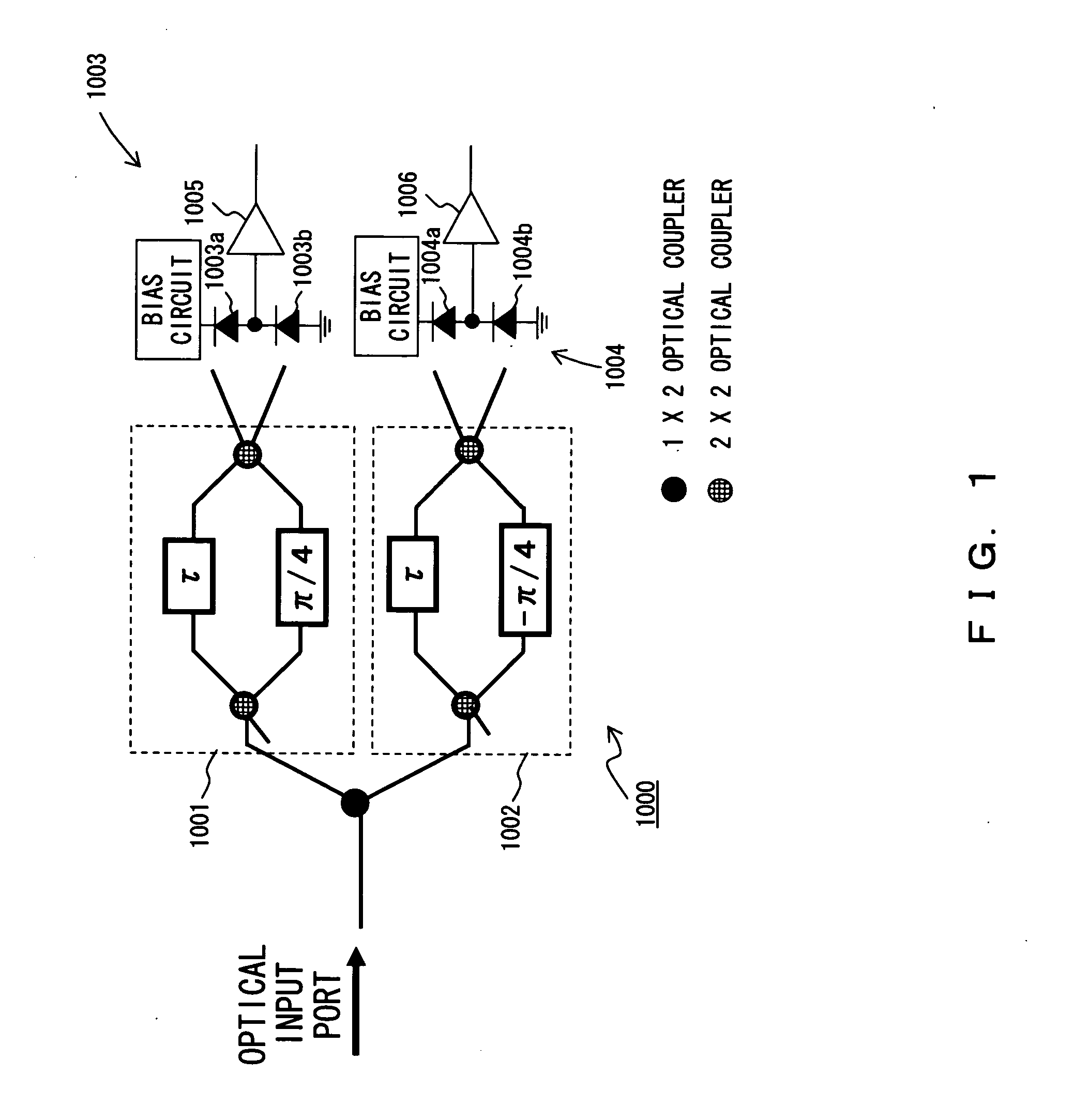
[0035]FIG. 4 is a diagram describing a configuration of the optical DQPSK receiver apparatus of the first embodiment according to the present invention. This optical DQPSK receiver apparatus receives the optical DQPSK signal via the optical input port 601 shown in FIG. 3. The optical DQPSK signal is input to an interferometer 10.
[0036] The interferometer 10 is a Mach-Zehnder interferometer, for example, and comprises an optical splitter 11, a delay element 12, a phase shift element 13, and an optical coupler 14. An optical splitter 11 splits an input optical DQPSK signal and guides the split signals to an optical path 15 and an optical path 16. The splitting ratio of the optical splitter 1 is 1:1, and optical signals with equal optical power are transmitted via the optical path 15 and the optical path 16. The optical splitter 11 can be realized by a 1×2 optical coupler, for example.
[0037] The delay element 12 is provided in the optical path 15 and delays optical signals by one-sym...
second embodiment
[0064]FIG. 8 is a diagram showing a configuration of the optical DQPSK receiver apparatus of the second embodiment according to the present invention. The basic configuration of the optical DQPSK receiver apparatus of the second embodiment is the same as that of the optical DQPSK receiver apparatus of the first embodiment. However, the optical DQPSK receiver apparatus of the second embodiment comprises a two-bit A / D converter 51 as a recovery circuit.
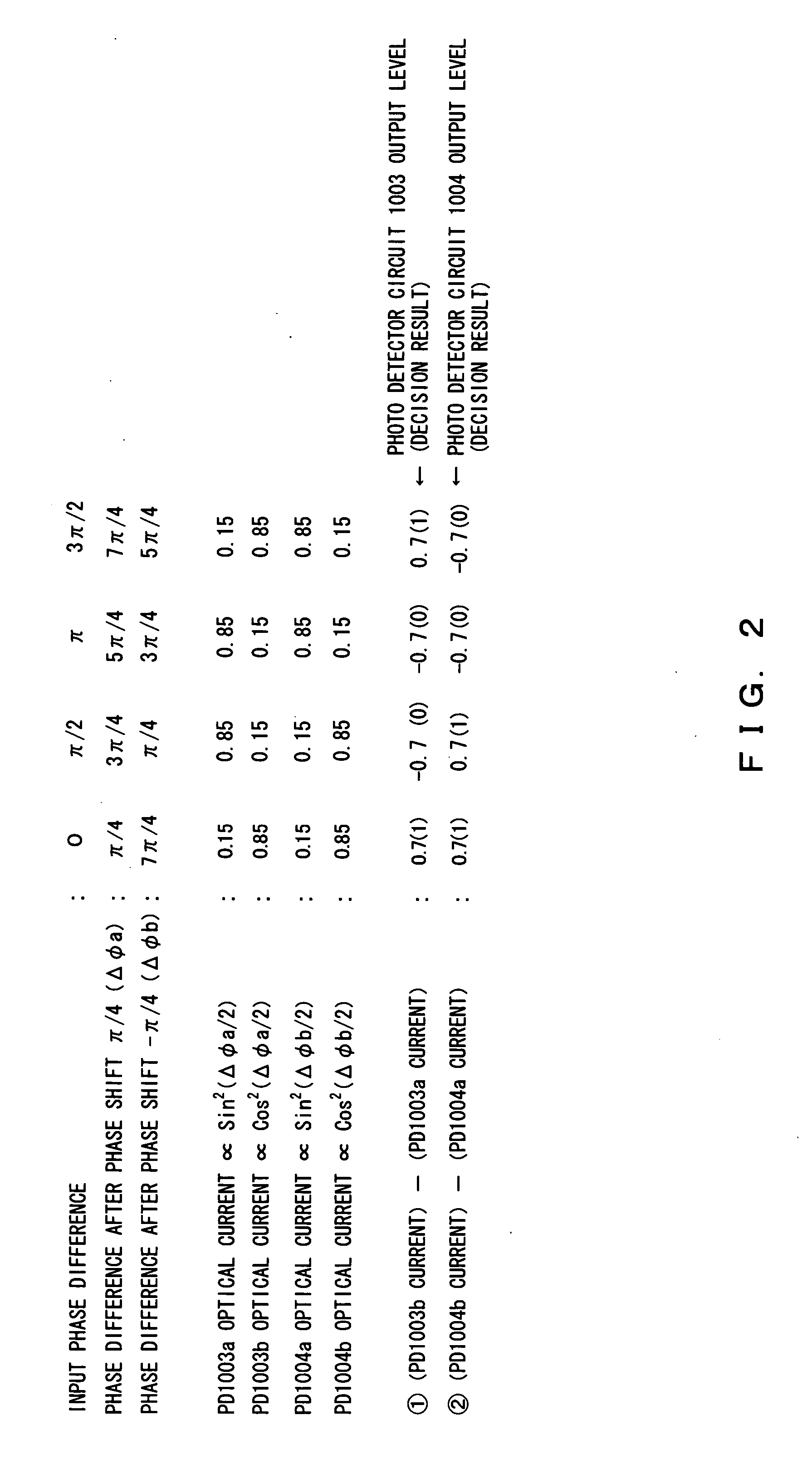
[0065] The two-bit A / D converter 51 converts the voltage of the detection signal output from the transimpedance amplifier 23 into two-bit digital data. At that time, the voltage of the detection signal is the same as that of the first embodiment and is determined in accordance with the phase difference between adjacent symbols. The two-bit A / D converter 51 is set so as to be able to discriminate each voltage value. In the example shown in FIG. 6, when the phase difference between adjacent symbols is “0”, “π / 2”, “π” or “3π / 2”, the volta...
third embodiment
[0068]FIG. 9 is a diagram showing the configuration of the optical DQPSK receiver apparatus of the third embodiment according to the present invention. The basic configuration of the optical DQPSK receiver apparatus of the third embodiment the same as the optical DQPSK receiver apparatus of the first embodiment. However, the optical DQPSK receiver apparatus of the third embodiment comprises a converter circuit 60 instead of the squaring circuit 32. The operations of the decision circuit 34 are different from those of the decision circuit 33.
[0069] The converter circuit 60 comprises diodes D1 and D2, a resistor R, and a capacitor C. The diodes D1 and D2 are connected in parallel and in an inverted orientation. The detection signal is provided to the anode of the diode D1 and the cathode of the diode D2. The cathode of the diode D1 and the anode of the diode D2 are grounded via the resistor R. The capacitor C removes the direct current component.
[0070] In the converter circuit 60 of...
PUM
 Abstract
Description
Claims
Application Information
PatSnap Eureka turns technology decisions into work you can execute. Powered by our Innovation Knowledge Graph, it runs expert workflows across engineering, life sciences, materials and intellectual property. Get your review-ready output in minutes.


