Method to improve the step coverage and pattern loading for dielectric films

Inactive Publication Date: 2007-10-04
APPLIED MATERIALS INC
View PDF54 Cites 626 Cited by
  • Summary
  • Abstract
  • Description
  • Claims
  • Application Information

AI Technical Summary

Benefits of technology

[0010]Embodiments of the present invention provide a method of controlling the step coverage and pattern loading of a layer on a substrate. In one embodiment, the method comprises placing a substrate with at least one formed feature across a surface of the substrate into a chamber. A dielectric layer

Problems solved by technology

However, it is often difficult to achieve conformal deposition.
For example, it is difficult to deposit a barrier layer over a feature with few or no resulting surface defects or feature deformation.
The non-uniformity of film

Method used


Image

  • Method to improve the step coverage and pattern loading for dielectric films
  • Method to improve the step coverage and pattern loading for dielectric films
  • Method to improve the step coverage and pattern loading for dielectric films

Examples


Embodiment Construction

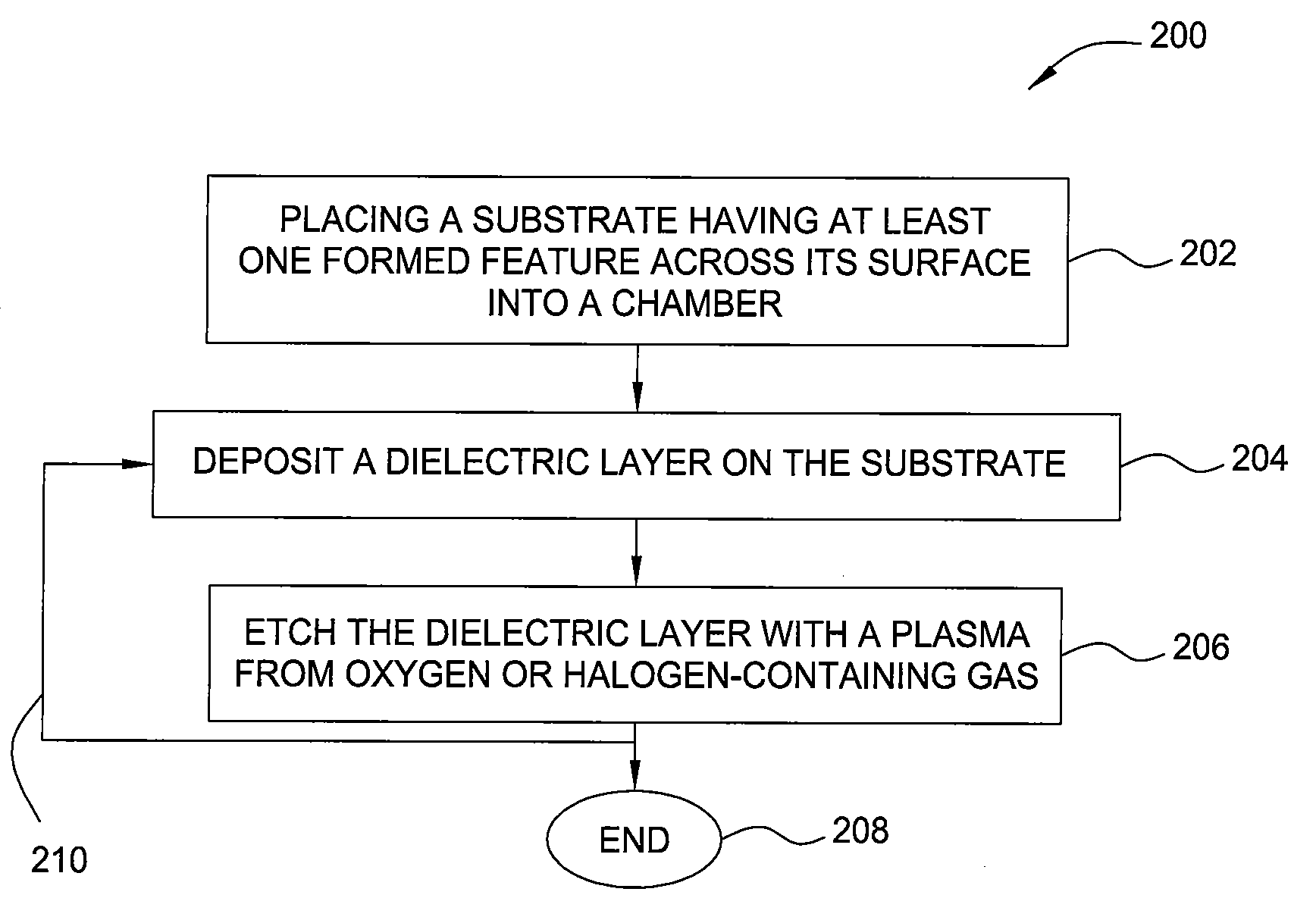
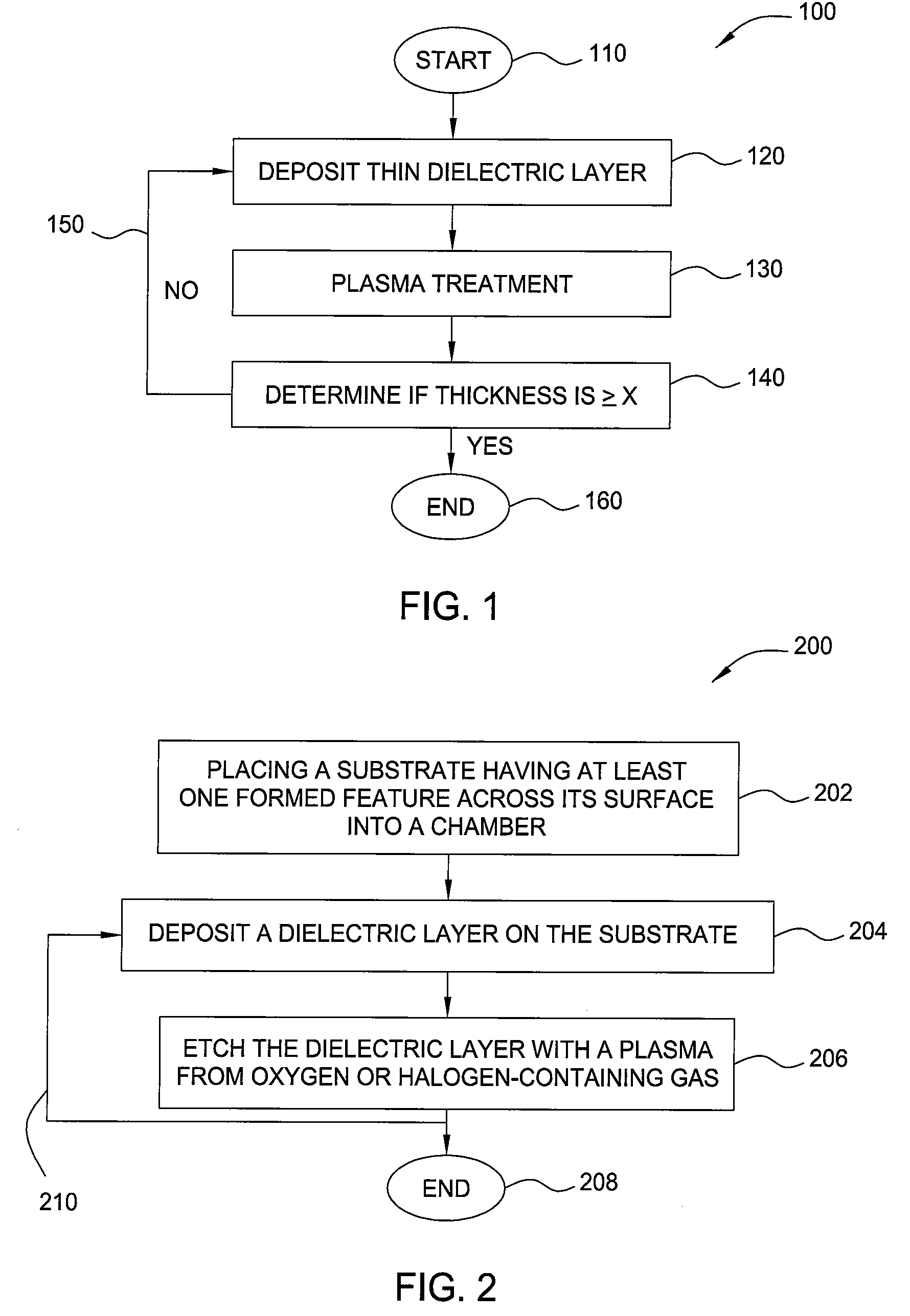
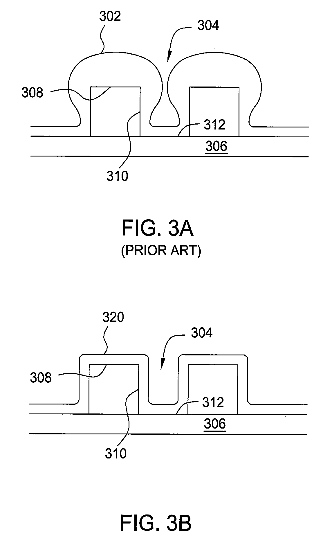
[0022]The present invention provides a method and apparatus for depositing a conformal dielectric layer over a formed feature. Films that can benefit from this process include dielectric materials such as silicon oxide, silicon oxynitride, or silicon nitride films that may be used as spacers or etch stop layers, for example. The films may be carbon doped, hydrogen doped, or contain some other chemical or element to tailor the dielectric properties. The film may be carbon doped or nitrogen doped. For example, the films may be SiCN, SiOC, SiOCN, SiBN, SiBCN, SiC, BN, or BCN films. In one aspect, a combination of thin layers that have been individually deposited and plasma treated provide a more conformal dielectric layer than a single thick dielectric layer. The chambers that may be used for the processes described herein include the PRODUCER® P3 chamber, PRODUCER® APF™ PECVD chamber, PRODUCER® BLACK DIAMOND® PECVD chamber, PRODUCER® BLOK® PECVD chamber, PRODUCER® DARC PECVD chamber, ...


PUM

PropertyMeasurementUnit
Fractionaaaaaaaaaa
Timeaaaaaaaaaa
Timeaaaaaaaaaa

Abstract

Methods of controlling the step coverage and pattern loading of a layer on a substrate are provided. The dielectric layer may be a silicon nitride, silicon oxide, or silicon oxynitride layer. The method comprises depositing a dielectric layer on a substrate having at least one formed feature across a surface of the substrate and etching the dielectric layer with a plasma from oxygen or a halogen-containing gas to provide a desired profile of the dielectric layer on the at least one formed feature. The deposition of the dielectric layer and the etching of the dielectric layer may be repeated for multiple cycles to provide the desired profile of the dielectric layer.

Description

CROSS-REFERENCE TO RELATED APPLICATIONS[0001]This application claims benefit of U.S. provisional patent application Ser. No. 60 / 788,279, filed Mar. 31, 2006, which is herein incorporated by reference.BACKGROUND OF THE INVENTION[0002]1. Field of the Invention[0003]Embodiments of the present invention generally relate to a method and apparatus for semiconductor processing. Specifically, embodiments of the present invention relate to a method and apparatus for depositing a conformal dielectric layer.[0004]2. Description of the Related Art[0005]Forming dielectric layers on a substrate by chemical reaction of gases is one of the primary steps in the fabrication of modern semiconductor devices. These deposition processes include chemical vapor deposition (CVD) as well as plasma enhanced chemical vapor deposition (PECVD), which uses plasma in combination with traditional CVD techniques.[0006]CVD and PECVD dielectric layers can be used as different layers in semiconductor devices. For examp...

Claims


Application Information

Patent Timeline
IPC IPC(8): H01L21/465
CPCH01L21/31116H01L21/76834H01L21/3185H01L21/02123H01L21/02274
Inventor BALSEANU, MIHAELAXIA, LI-QUNSHEK, MEI-YEEM'SAAD, HICHEM
Owner APPLIED MATERIALS INC
Why Eureka
Try Eureka