Plasma display panel and process for producing the plasma display panel
a technology of plasma display panel and plasma, which is applied in the manufacture of electric discharge tubes/lamps, electrodes, and electrode systems. it is difficult and expensive to form fluoride film, and the film has a poor uv transmittance, so as to reduce the uv transmission, reduce the uv, and reduce the uv. the effect of reducing the uv transmission
- Summary
- Abstract
- Description
- Claims
- Application Information
AI Technical Summary
Benefits of technology
Problems solved by technology
Method used
Image
Examples
first embodiment
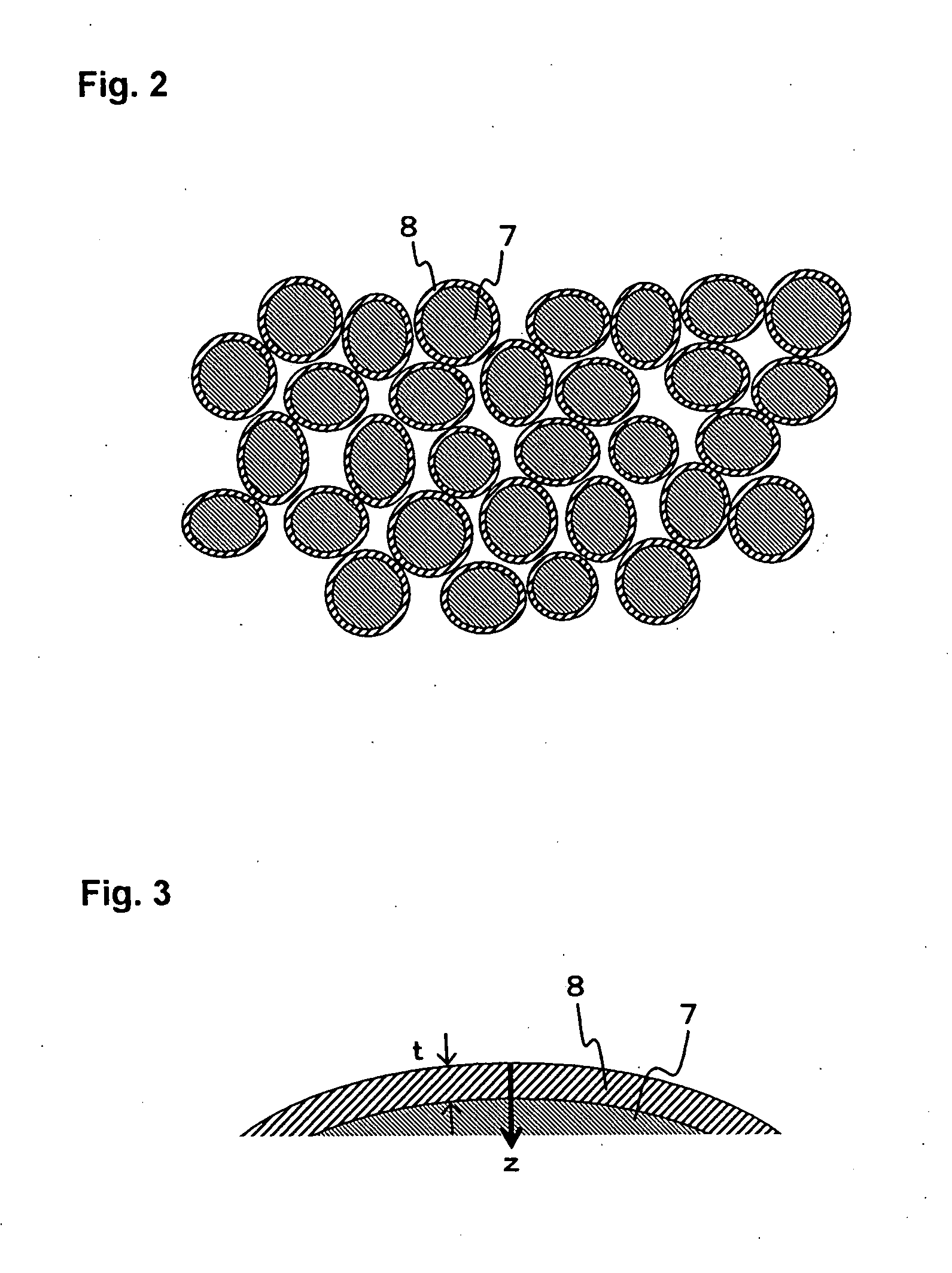
[0088] This embodiment relates to a PDP and a process for producing it in which an entire surface of each phosphor particle is covered with a coating made of a fluoride such as magnesium fluoride.
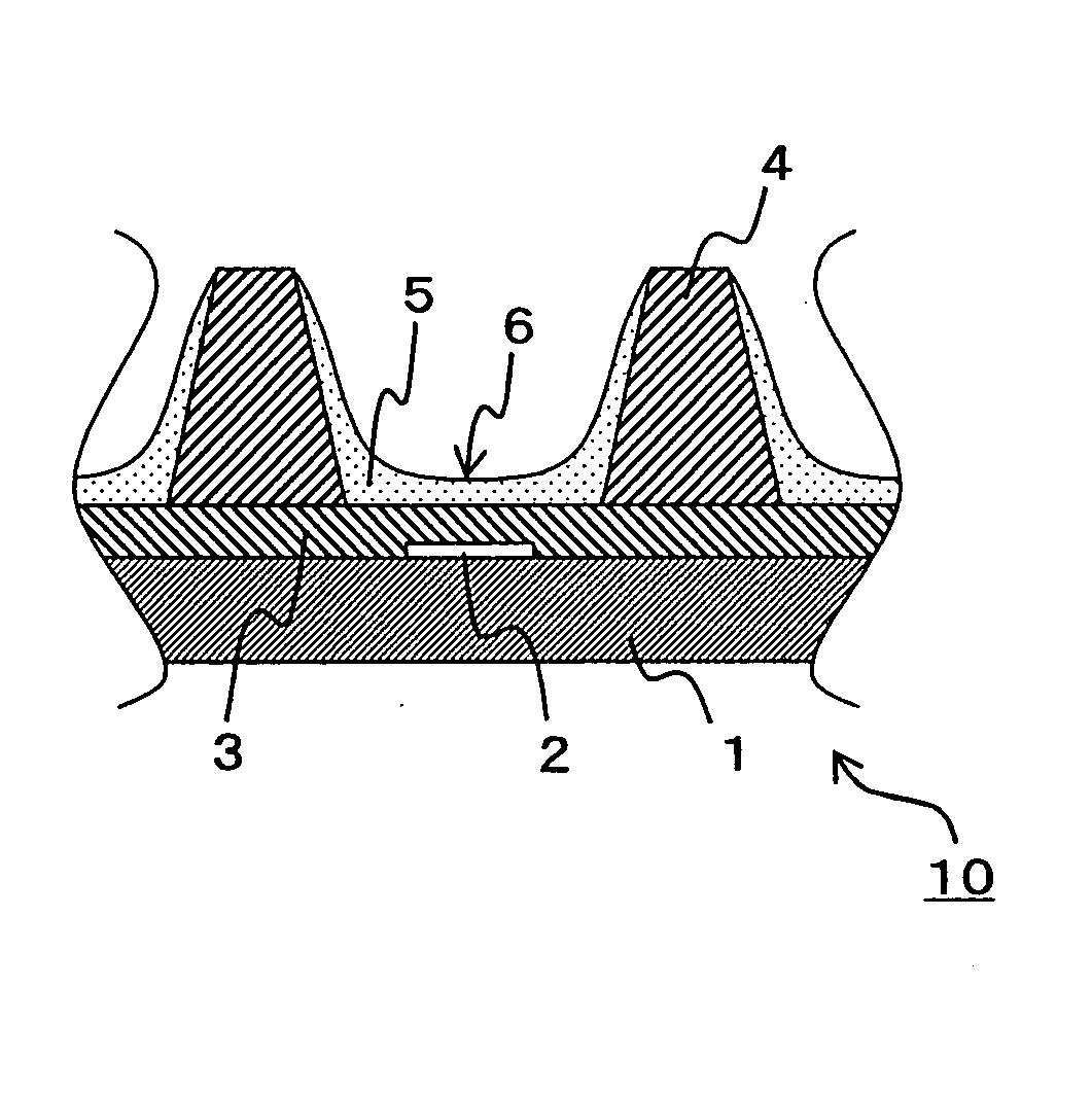
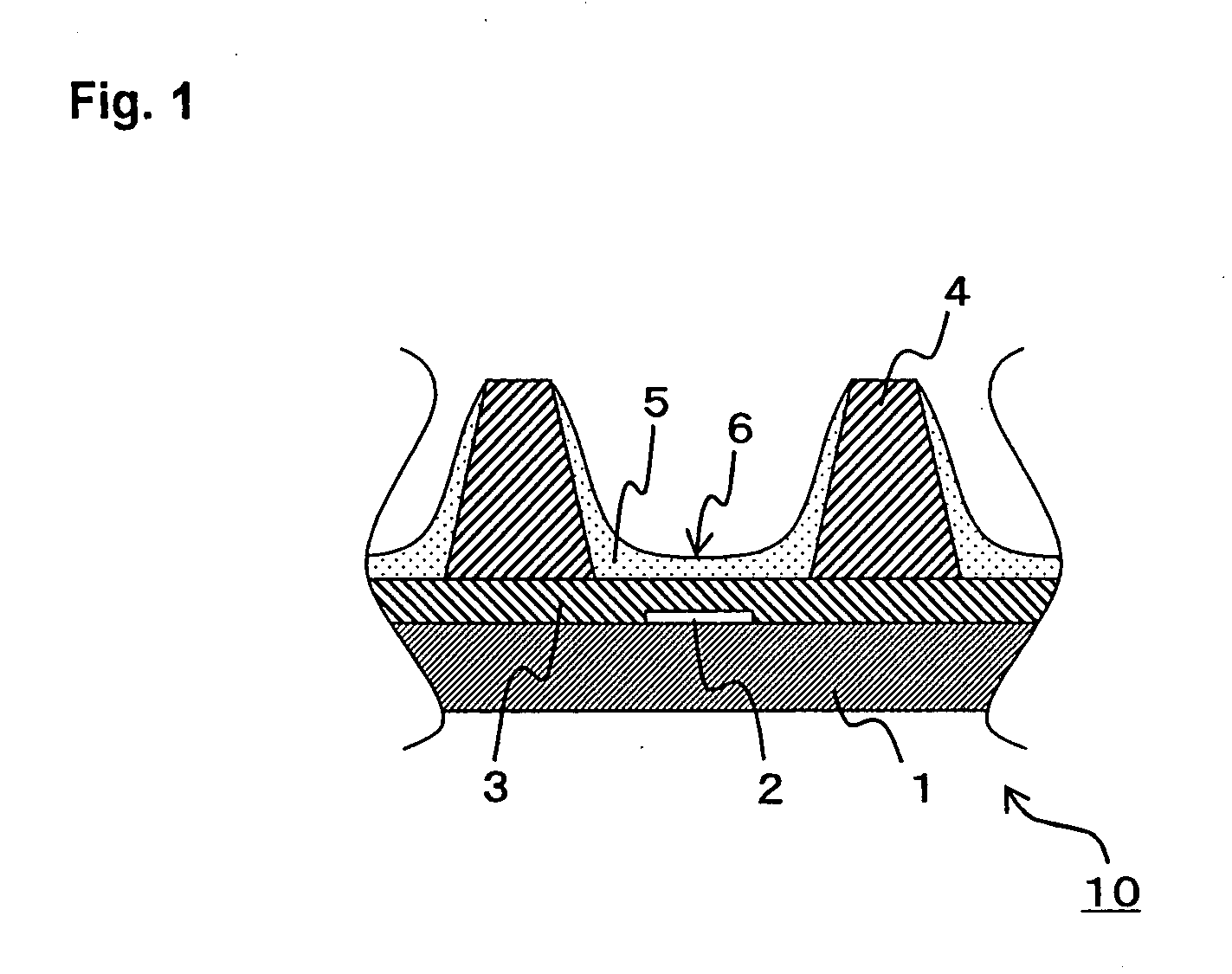
[0089] A PDP of the present embodiment is constructed by positioning a rear plate 10 shown in FIG. 1 to be opposed to a front plate (not shown) and form discharge spaces therebetween while locating a phosphor layer 6 inside the spaces, and by filling the discharge spaces with a discharge gas. In the rear plate 10, address electrodes 2 (one of which is shown in FIG. 1) are located on a rear substrate 1 which is generally made of glass, and a dielectric layer 3 covers the rear substrate 1 with the address electrodes 2. A plurality of ribs 4 is located on the dielectric layer 3 and each address electrode 2 is situated between the adjacent ribs 4. A phosphor layer 5 is formed between the adjacent ribs on a surface of the dielectric layer 3 covering the rear substrate 1 (as well as on side wall...
second embodiment
[0117] This embodiment relates to a PDP and a process for producing it in which an entire surface of each phosphor particle is covered with a coating made of a fluoride-containing phosphor substance.
[0118] A PDP of the present embodiment may have a similar structure to that of the PDP of the first embodiment described above with reference to FIGS. 1 to 3, except for a material of a coating. A coating in the present embodiment is made of a fluoride-containing phosphor substance. In a case for a blue phosphor particle, for example, the coating includes atoms of fluorine, europium, barium, aluminum, magnesium and oxygen. In a case for a red phosphor particle, the coating includes atoms of fluorine, europium, yttrium and oxygen. In a case for a green phosphor particle, the coating includes atoms of fluorine, manganese, barium, aluminum and oxygen.
[0119] A thickness of the coating is preferably about 1 to 5 nm. A coating having a thickness less than 1 nm cannot be formed with high repr...
third embodiment
[0125] This embodiment relates to a PDP and a process for producing it in which an entire surface of each phosphor particle is covered with a coating made of a fluorine-added silicon oxide layer and a silicon oxide layer.
[0126] A PDP of the present embodiment may have a similar structure to that of the PDP of the first embodiment described above with reference to FIG. 1, except for a material and a structure of a coating. As shown in FIGS. 7 and 8, a coating in the present embodiment is made of a fluorine-added silicon oxide (SiOF) layer 11 and a silicon oxide (SiO2) layer 12 thereon.
[0127] A thickness of the fluorine-added silicon oxide layer 11 of coating 8′ is preferably about 1 to 20 nm and more preferably about 1 to 15 nm. A thickness of the silicon oxide layer 12 of the coating 8′ is preferably about 1 to 10 nm and more preferably about 1 to 5 nm. With respect to both layers, a layer having a thickness less than 1 nm cannot be formed with high reproducibility and cannot prov...
PUM
| Property | Measurement | Unit |
|---|---|---|
| diameter | aaaaa | aaaaa |
| diameter | aaaaa | aaaaa |
| diameter | aaaaa | aaaaa |
Abstract
Description
Claims
Application Information
 - R&D
- Intellectual Property
- Life Sciences
- Materials
- Tech Scout
- Unparalleled Data Quality
- Higher Quality Content
- 60% Fewer Hallucinations
Browse by: Latest US Patents, China's latest patents, Technical Efficacy Thesaurus, Application Domain, Technology Topic, Popular Technical Reports.
© 2025 PatSnap. All rights reserved.Legal|Privacy policy|Modern Slavery Act Transparency Statement|Sitemap|About US| Contact US: help@patsnap.com


