Non-Linear Terahertz Spectroscopy for Defect Density Identification in High K Dielectric Films

a defect density and terahertz spectroscopy technology, applied in the field of performing terahertz (thz) spectroscopy, can solve the problems of gate leakage, limiting the operation range of the device, and affecting the performance of the device,

Inactive Publication Date: 2007-10-11
NEW JERSEY INSTITUTE OF TECHNOLOGY
View PDF9 Cites 36 Cited by
  • Summary
  • Abstract
  • Description
  • Claims
  • Application Information

AI Technical Summary

Benefits of technology

[0011] In accordance with the present invention, methods are disclosed to infer the density of defects in high K dielectric films in a non-contact, non-invasive and non-destructive manner. THz radiation is employed to measure the change in electrical conductivity of the films before and after illumination with visible light, where the visible light photoionizes the defects thereby changing the electrical conductivity and changing ...

Problems solved by technology

However, the silicon-based microelectronics industry is rapidly approaching the point where device performance is compromised by feature size.
Specifically, the gate dielectric based on SiO2 scaled to a node size of 90 nm will not insulate well enough, thereby leading to gate leakage.
Current MOSFET technology with 1.3 nm thick SiO2 as the gate dielectric material portrays high gate leakage and reduced drive currents, thus limiting the o...

Method used


Image

  • Non-Linear Terahertz Spectroscopy for Defect Density Identification in High K Dielectric Films
  • Non-Linear Terahertz Spectroscopy for Defect Density Identification in High K Dielectric Films
  • Non-Linear Terahertz Spectroscopy for Defect Density Identification in High K Dielectric Films

Examples


Embodiment Construction

[0050] In the following description, for purposes of explanation, specific numbers, materials and configurations are set forth in order to provide a thorough understanding of the invention. It will be apparent, however, to one having ordinary skill in the art that the invention may be practiced without these specific details. In some instances, well-known features may be omitted or simplified so as not to obscure the present invention. Furthermore, reference in the specification to phrases such as “one embodiment” or “an embodiment” means that a particular feature, structure or characteristic described in connection with the embodiment is included in at least one embodiment of the invention. The appearances of phrases such as “in one embodiment” in various places in the specification are not necessarily all referring to the same embodiment.

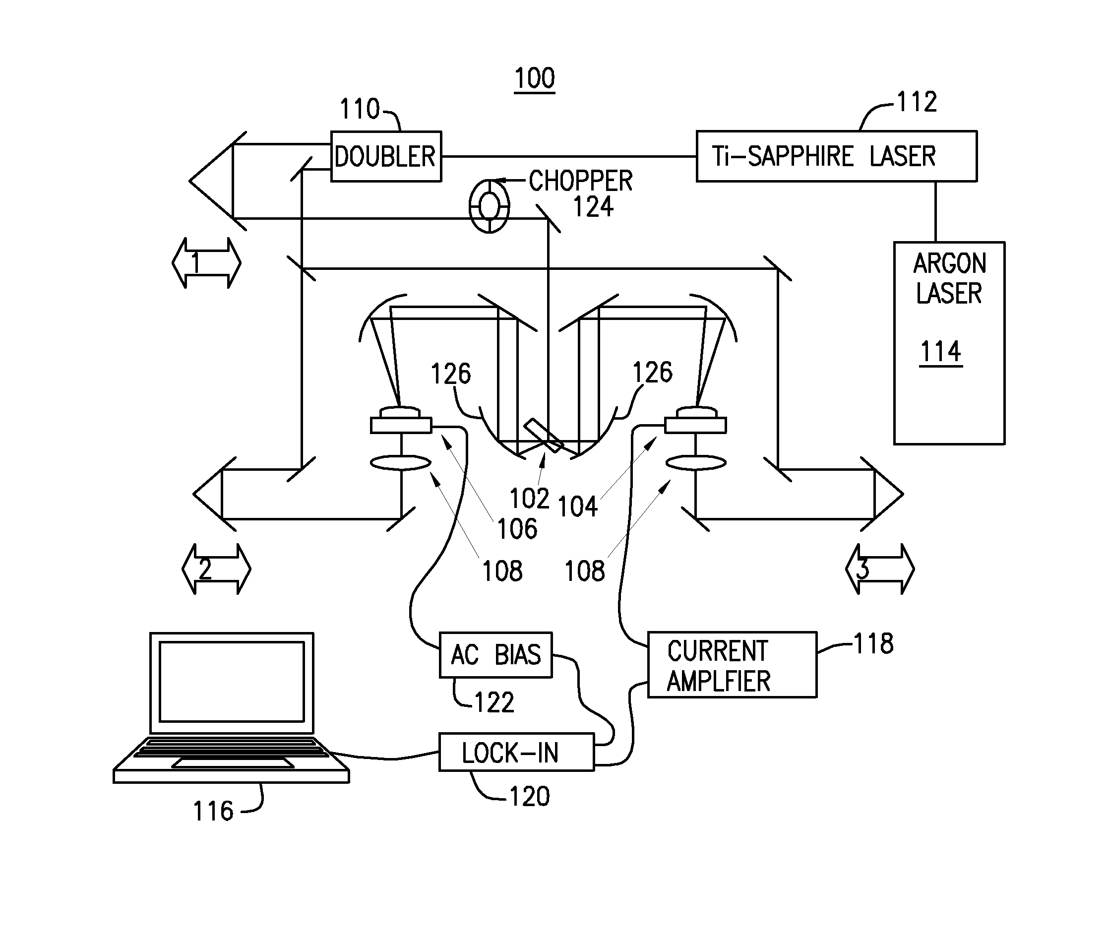
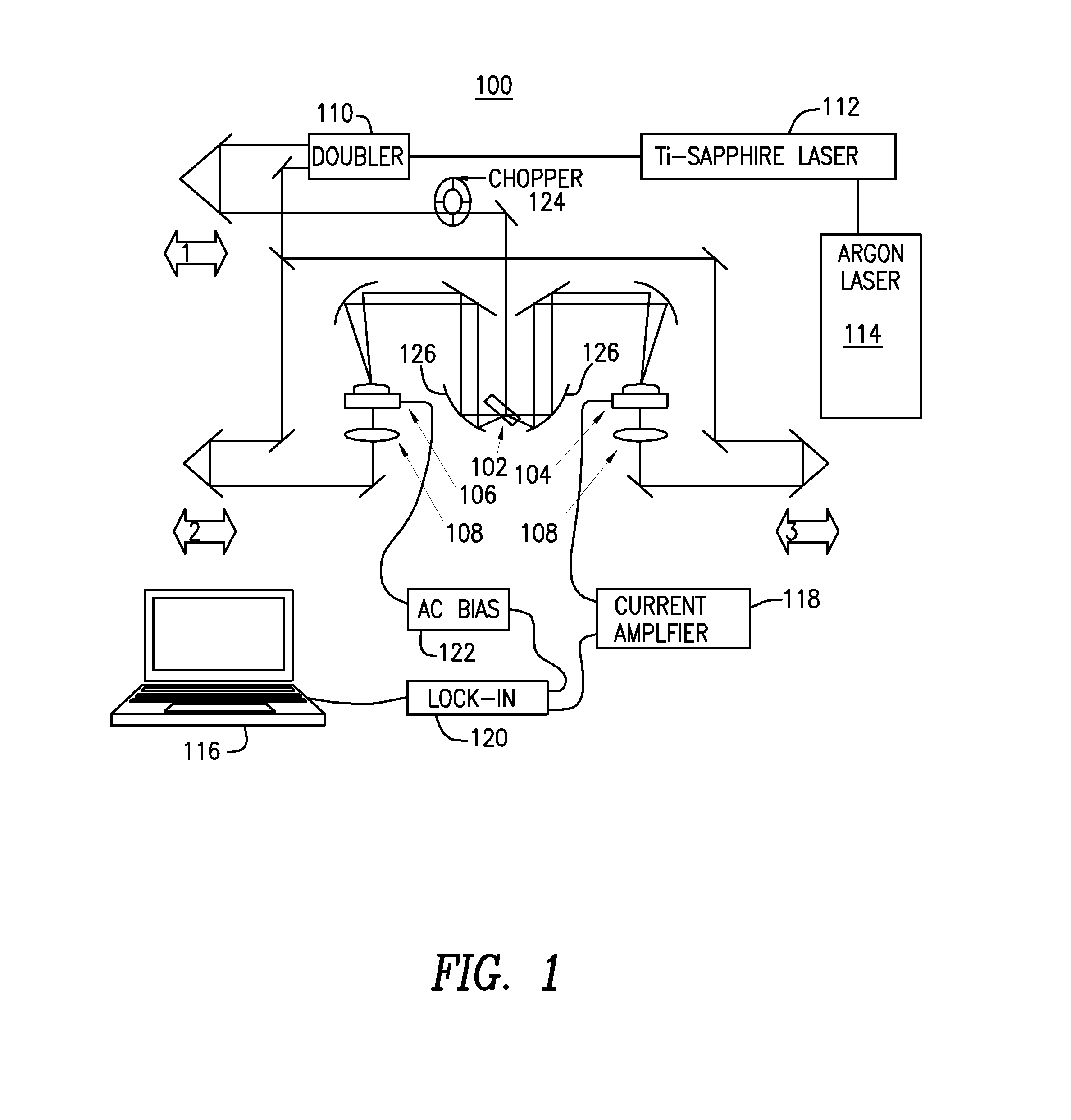
[0051] Characterization of HfO2 and SiO2 on p-type silicon, 200 mm diameter substrates using Terahertz (THz) transmission with and without optic...


PUM


Abstract

Methods to infer the density of defects in high κ dielectric films in a non-contact, non-invasive and non-destructive manner. THz radiation is employed to measure the change in electrical conductivity of the films before and after illumination with visible light, where the visible light photoionizes the defects thereby changing the electrical conductivity and changing the transmission (or reflection) of THz radiation from the films. The disclosed techniques can be employed to make measurements as soon as wafers are fabricated. The technology is applicable to wafers of any size.

Description

CROSS-REFERENCE TO RELATED APPLICATIONS [0001] This Application claims the benefit of U.S. Provisional Patent Application Ser. No. 60 / 789,683, filed Apr. 6, 2006, entitled “Non-Linear Terahertz Spectroscopy for Defect Density Identification in High K Dielectric Films”, the entire disclosure of which is incorporated by reference herein.BACKGROUND OF THE INVENTION [0002] 1. Field of the Invention [0003] This invention relates to a method and apparatus for performing terahertz (THz) spectroscopy and, more particularly, for optically pumping and THz probing a sample object under test by a non-linear technique. [0004] 2. Description of the Related Art [0005] Over the years, the trend towards smaller scales in Metal-Oxide Semiconductor Field-Effect Transistors (MOSFETs) and other CMOS based technologies has brought about substantial improvements in devices performance. However, the silicon-based microelectronics industry is rapidly approaching the point where device performance is comprom...

Claims


Application Information

Patent Timeline
IPC IPC(8): G01J5/02
CPCG01J3/42G01N21/3581G01N21/3563G01N21/9501G01N21/636
Inventor FEDERICI, JOHN FRANCISGREBEL, HAIMALTAN, HAKAN
Owner NEW JERSEY INSTITUTE OF TECHNOLOGY
Why Eureka
Try Eureka