Program and Erase Methods with Substrate Transient Hot Carrier Injections in a Non-Volatile Memory

a non-volatile memory and hot carrier technology, applied in static storage, digital storage, instruments, etc., can solve the problems of large vt distribution of erase state, charge loss, and erase time must be increased gradually, so as to reduce the operation bias voltage and shorten the operation time. , the effect of uniform channel program and erase characteristics

Inactive Publication Date: 2007-10-11
MACRONIX INT CO LTD
View PDF21 Cites 14 Cited by
  • Summary
  • Abstract
  • Description
  • Claims
  • Application Information

AI Technical Summary

Benefits of technology

[0019]Advantageously, the present invention provides program and erase methods suitable for SONOS-type or FG-type memory devices with a lower operation bias voltage as well as a shorter operation time. The present invention also advantageously produces uniform channel program and erase characteristics from the substrate transient hot electron injection and the substrate transient hot hole injection. The present invention also advantageously produces desirable cycle endurance and data retention qualities.

Problems solved by technology

However, the hot hole injection causes oxide damage, leading to charge loss in the high threshold cell and charge gain in the low threshold cell Moreover, the erase time must be increased gradually during program and erase cycling due to the hard-to-erase accumulation of charge in the charge trapping structure.
This difference in erase speed results in a large Vt distribution of the erase state, where some of the cells become hard to erase and some of them are over-erased.
Thus the target threshold Vt window is closed after many program and erase cycles and poor endurance is observed.
This phenomenon will become more serious as the technology continues to scale down.
Evaluating the endurance and retention of an nitride read-only memory array, the lack of uniformity in eraseability causes a margin loss due to cycling and baking.
In a subsequent erase operation using a technique such as BTBTHH, it would be difficult to move holes toward the middle of the channel region which makes the residual electrons located near the channel region hard to erase.
In comparison with traditional SONOS memory with a thin tunneling oxide, a thicker bottom oxide is selected to achieve better data retention, but the thicker bottom oxide is not desirable for a NAND-type nitride trapped memory application.
A drawback of the FN tunneling technique is the extremely low FN tunneling rate of electrons and holes.

Method used


Image

  • Program and Erase Methods with Substrate Transient Hot Carrier Injections in a Non-Volatile Memory
  • Program and Erase Methods with Substrate Transient Hot Carrier Injections in a Non-Volatile Memory
  • Program and Erase Methods with Substrate Transient Hot Carrier Injections in a Non-Volatile Memory

Examples


Embodiment Construction

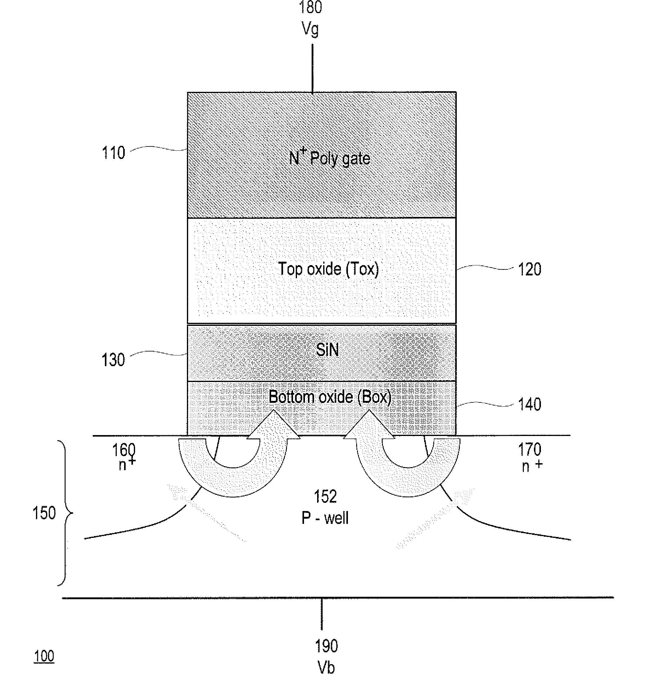
[0032]Referring now to FIG. 1, there is shown a simplified structural diagram illustrating a charge trapping memory cell 100 for carrying out a substrate transient hot carrier injection in a SONOS cell. The charge trapping memory cell 100 has a substrate 150 with n+ doped regions 160 and 170, and a p-doped region 152 between the n+ doped regions 160 and 170. A bottom dielectric structure 140 (bottom oxide) overlays the substrate 150; a charge trapping structure 130 (e.g. silicon nitride layer) overlays the bottom dielectric structure 140; a top dielectric structure (top oxide) 120 overlays the charge trapping structure 130; and an n+ poly gate 110 overlays the top dielectric structure 120. A gate voltage 180, Vg, is applied to the n+ poly gate 110, and a body voltage 190, Vb, is applied to the P-well substrate 150. Representative top dielectrics include silicon dioxide and silicon oxynitride having a thickness of about 5 to 10 nanometers, or other similar high dielectric constant ma...


PUM


Abstract

The present invention describes a uniform program method and a uniform erase method of a charge trapping memory by employing a substrate transient hot electron technique for programming, and a substrate transient hot hole technique for erasing, which emulate an FN tunneling method for NAND memory operation. The methods of the present invention are applicable to a wide variety of charge trapping memories including n-channel or p-channel SONOS types of memories and floating gate (FG) type memories. the programming of the charge trapping memory is conducted using a substrate transient hot electron injection in which a body bias voltage Vb has a short pulse width and a gate bias voltage Vg has a pulse width that is sufficient to move electrons from a channel region to a charge trapping structure.

Description

REFERENCE TO RELATED APPLICATION[0001]This application claims the benefit of U.S. Provisional Patent Application No. 60 / 789,767, filed 6 Apr. 2006 by inventors Tzu Hsuan Hsu, Chao I Wu, Kuang Yeu Hsieh and Yan Chin King, entitled Program and Erase Methods with Substrate Transient Hot Carrier Injections in a Non-Volatile Memory.BACKGROUND OF THE INVENTION[0002]1. Field of the Invention[0003]The present invention relates generally to electrically programmable and erasable memory, and more particularly, to injecting hot carriers in non-volatile memories.[0004]2. Description of Related Art[0005]Electrically programmable and erasable non-volatile memory technologies based on charge storage structures known as Electrically Erasable Programmable Read-Only Memory (EEPROM) and flash memory are used in a variety of modern applications. A flash memory is designed with an array of memory cells that can be independently programmed and read. Sense amplifiers in a flash memory are used to determin...

Claims


Application Information

Patent Timeline
Patent Type & Authority Applications(United States)
IPC IPC(8): G11C16/02
CPCG11C16/0466
Inventor HSU, TZU HSUANWU, CHAO-IHSIEH, KUANG YEUKING, YA-CHIN
Owner MACRONIX INT CO LTD
Why Eureka
Try Eureka