

Schottky Gate Organic Field Effect Transistor and Fabrication Method of the Same
a technology of organic field effect transistor and organic gate, which is applied in the direction of solid-state devices, semiconductor devices, thermoelectric devices, etc., can solve the problems of low current (isd) between the source and drain, the fabrication method of the transistor cannot be fully taken advantage of, and the operating voltage is relatively high
- Summary
- Abstract
- Description
- Claims
- Application Information
AI Technical Summary
Benefits of technology
Problems solved by technology
Method used
Image

Examples
embodiment 1
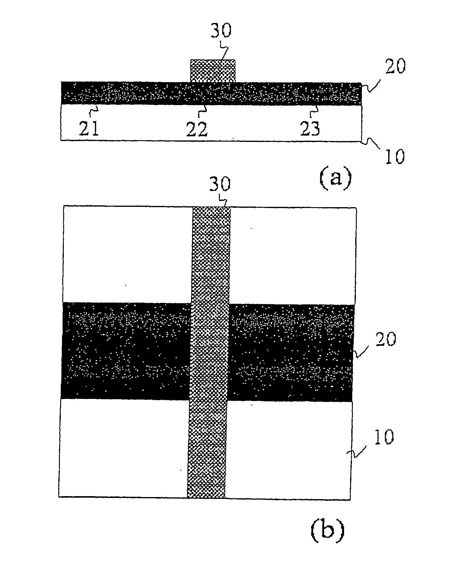
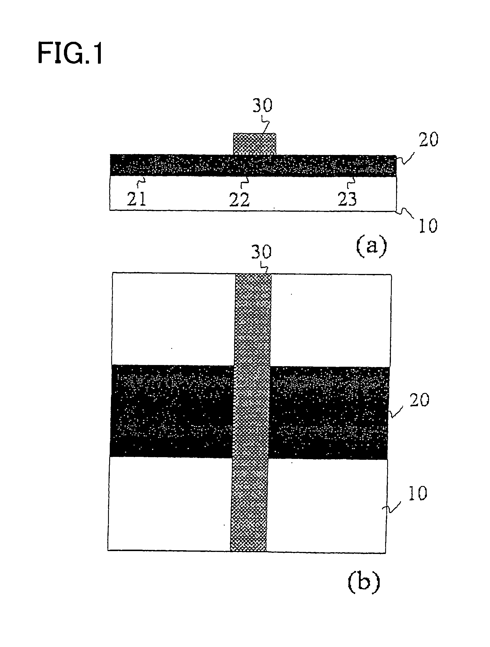
[0062]FIG. 1 (a) illustrates a top gate type (the working electrode as a gate is on the channel) structure of Schottky gate organic field effect transistors. The source 21, channel 22 and drain 23 are fabricated on the substrate 10 that has at least an insulating surface. The source 21, channel 22 and drain 23 are made using the same organic conductive material, and are in a continuous structure. A 100 μm thick PET (poly(ethyleneterephthalate)) film is used for the substrate 10, and poly(3,4-ethylenedioxythiophene) doped with poly(4-styrenesulfonate) is used for the source 21, channel 22 and drain 23.
[0063] The gate electrode 30 is formed on the region of the channel 22 by vacuum deposition. The gate electrode 30 is formed in a strip on the region of the channel 22. The width of the channel 22 is 1 mm, the length is 100 μm, the height is from 25 to 40 μm. FIG. 1 (b) is a plan view of the transistor.
[0064] In the embodiment, polyethylene terephthalate (PET, 100 μm thick OHP film, T...
case 1
(Examination Examination of the Contact State of an Interface)
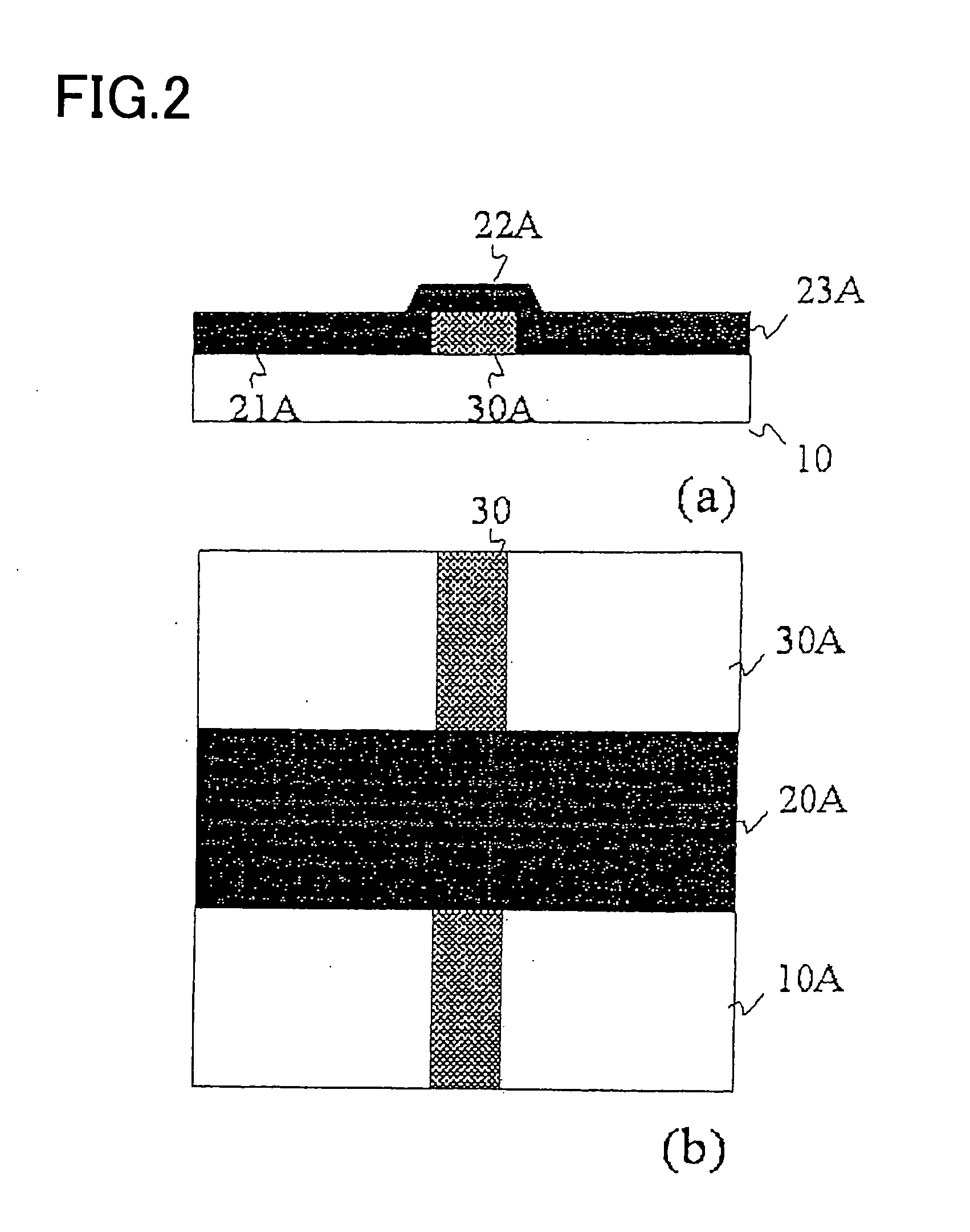
[0083]FIG. 8 is graphs showing the relationship between average surface roughness Ra and contact state of interface. Polyethylene terephthalate (PET, 100 μm thick OHP film, Tochiman Co. Ltd.) was used as a substrate, on which PEDOT / PSS was applied as an organic conductor, then the surface was processed so that the average surface roughness Ra was 2.5 mm or less, and an Al gate electrode was formed on the surface by a vapor deposition method. It has been confirmed from the voltage-current characteristics shown in FIG. 8 (a) that the contact between the organic conductor and the Al electrode was a Schottky contact.
[0084]FIG. 8 (b) shows the result of using a substrate and an organic conductor in the same way as above, then processing the surface of the organic conductor so that the average surface roughness Ra should be 3 mm or more, and forming an Al gate electrode on the surface by a vapor deposition method. It has been...
case 2
(Examination Examination of a Field Mobility μ and a Carrier Density (NA))
[0085] An examination was performed on the carrier density of the source, channel and drain of the Schottky gate organic field effect transistor having a top gate type structure fabricated in Embodiment 1. In the conventional organic field effect transistor using an amorphous organic semiconductor for the channel, it is known that the relationship represented by Formula 1 is established between the conductivity (σ) and the carrier field mobility (μ).
μ∂σδ(δ=0.76) Formula 1
[0086] Thus, the relationship is established that the field mobility (μ) increases in proportion to the conductivity (σ) in a wide region of the conductivity ranging from 10−7 to 10−1 S / cm.
[0087] Furthermore, it is known that the relationship represented by Formula 2 is established between the conductivity (σ) and the dopant concentration (Nd), and that the relationship represented by Formula 3 is established among the conductivity (σ) of...
PUM
| Property | Measurement | Unit |
|---|---|---|
| Area | aaaaa | aaaaa |
| Nanoscale particle size | aaaaa | aaaaa |
| Surface roughness | aaaaa | aaaaa |
Abstract
Description
Claims
Application Information