

Voltage Level Shifter
a voltage level shifter and shifter technology, applied in pulse manipulation, pulse technique, instruments, etc., can solve the problems of high manufacture cost and increase in manufacturing cost of voltage level shifters, and achieve the effect of saving power and simplifying manufacturing processes
- Summary
- Abstract
- Description
- Claims
- Application Information
AI Technical Summary
Benefits of technology
Problems solved by technology
Method used
Image

Examples
second embodiment
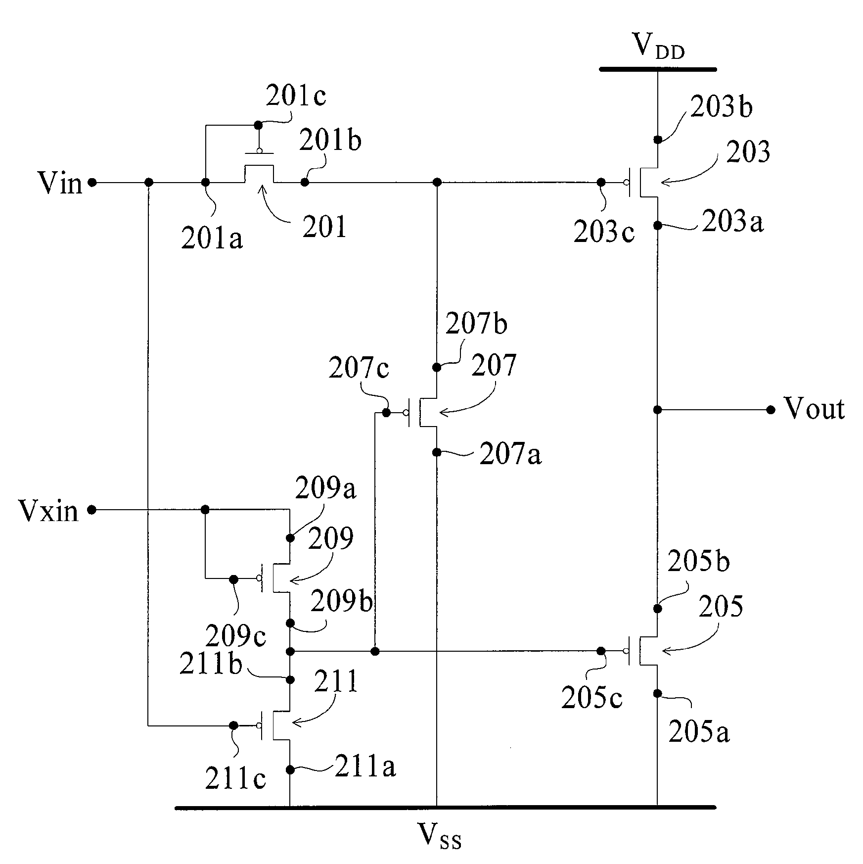
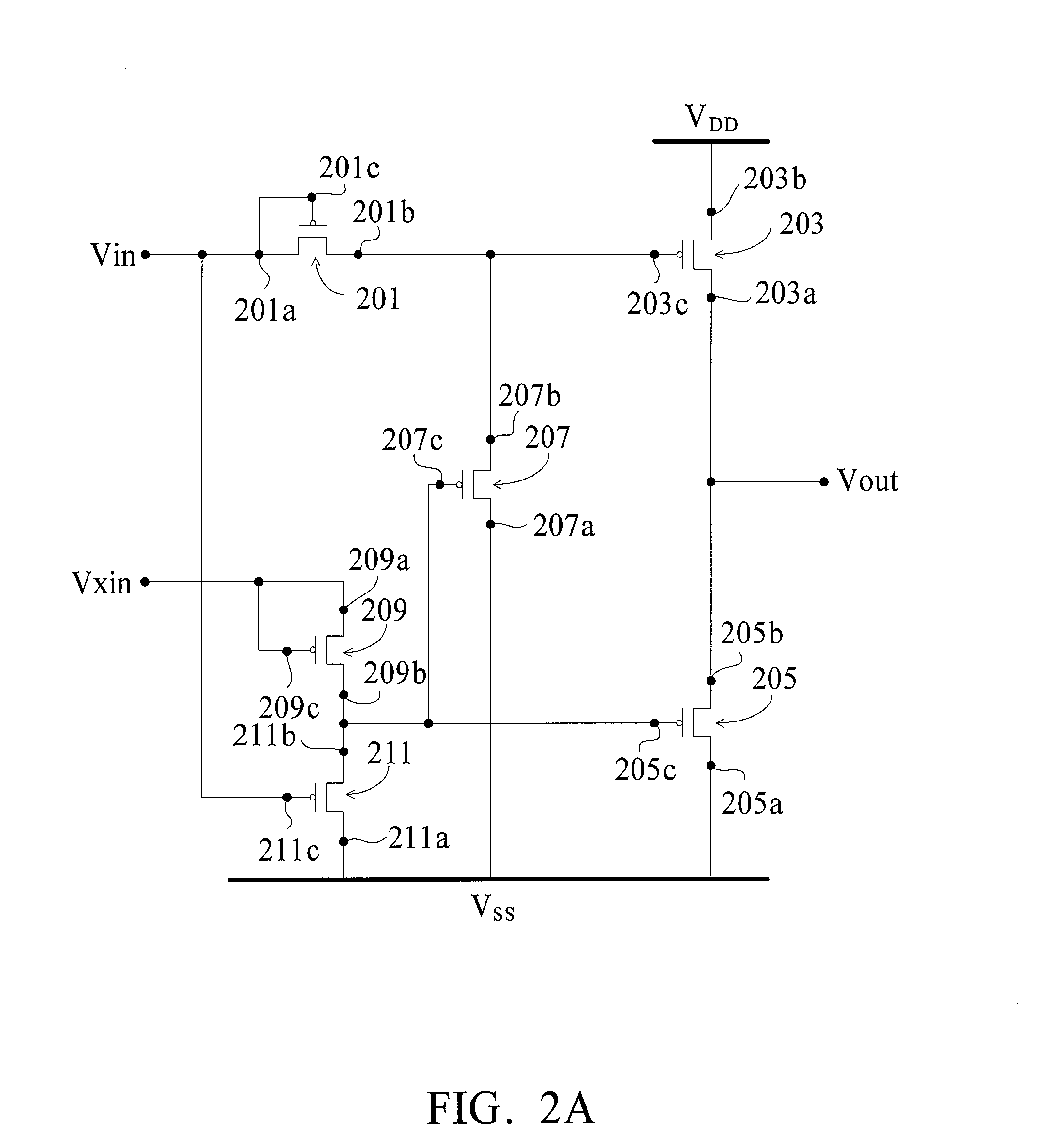
[0028]FIG. 3A shows the present invention, which comprises a first input terminal Vin, a second input terminal Vxin, an output terminal Vout, a first power supply terminal VDD, a second power supply terminal VSS, a first input unit 31, a second input unit 33, a first TFT 301, a disable unit 35, a feedback unit 37, and a second TFT 303. The first input terminal Vin is configured to input a first input signal. The second input terminal Vxin is configured to input a second input signal. The output terminal Vout is configured to output an output signal. The first input signal and the second input signal are complementary, and the output signal of the output terminal Vout and the first input signal are substantially in phase. The connections among these elements are described below.
[0029]The first input unit 31 receives the first input signal via the first input terminal Vin, and outputs a first switching control signal 300. The second input unit 33, electrically coupled to the second po...
third embodiment
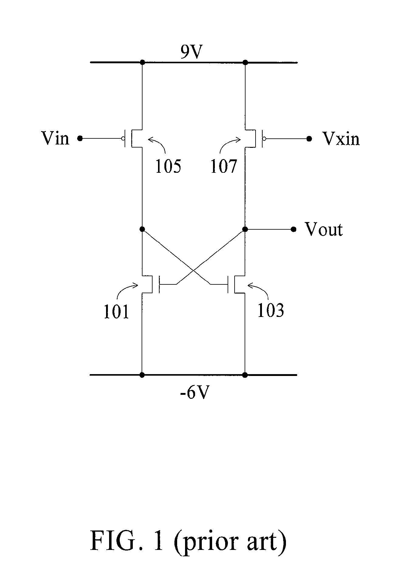
[0041]The eleventh TFT 401 and the twelfth TFT 403 cause a Bootstrap effect. They, as well as the thirteenth TFT 405 of the second input unit 33, are capable of improving the performance of the whole circuit. FIGS. 4B, 4C, and 4D show simulation voltage versus time waveforms of the first input terminal Vin and the output terminal Vout under three different TFT threshold voltages in accordance to the third embodiment, respectively. FIG. 4B shows the waveforms under a first threshold voltage, substantially −1V, FIG. 4C shows the waveforms under a second threshold voltage, substantially −2.5V, and FIG. 4D shows the waveforms under a third threshold voltage, substantially −4V. Meanwhile, the simulation conditions for deriving the waveforms in FIGS. 4B, 4C, and 4D are that: the first power supply terminal VDD is substantially equal to −6V, the second power supply terminal VSS is substantially equal to 9V, the first input terminal Vin swings from about 0V to about 5V, the electron mobilit...
fourth embodiment
[0046]FIGS. 5B, 5C, and 5D show simulation voltage versus time waveforms of the first input terminal Vin and the output terminal Vout under three different TFT threshold voltages in accordance to the fourth embodiment, respectively. FIG. 5B shows the waveforms under a first threshold voltage, substantially −1V, FIG. 5C shows the waveforms under a second threshold voltage, substantially −2.5V, and FIG. 5D shows the waveforms under a third threshold voltage, substantially −5V. Meanwhile, the simulation conditions for deriving the waveforms in FIGS. 5B, 5C, and 5D are that: the first power supply terminal VDD is substantially equal to −6V, the second power supply terminal VSS is substantially equal to 9V, the first input terminal Vin swings from about 0V to about 5V, the electron mobility of the PMOS TFTs is about 60 cm2 / Vsec, and an output load has about 20 pF capacitance. One can observe that the waveforms of the output terminal Vout are excellent no matter the threshold voltage is l...
PUM
 Abstract
Description
Claims
Application Information