Content addressable memory

Inactive Publication Date: 2007-10-25
RENESAS TECH CORP
View PDF3 Cites 54 Cited by
  • Summary
  • Abstract
  • Description
  • Claims
  • Application Information

AI Technical Summary

Benefits of technology

[0027]An object of the invention is to provide a content addressable memory that can reduce current

Problems solved by technology

Therefore, the search line has a large capacitive load.
Therefore, the charge and discharge currents of the search line and the match line are large, resulting in a problem that current dissipation and power consumption are large.
In the CAM and TCAM, as described above, the search line and the match line are charged and discharged in each search cycle, and the current consumption is large.
Therefore, a simultaneous operation current (peak current) is large, which may cause switching noises.
Therefore, signal amplitudes of the local and global match lines indicating a result of the match-detection are large, and such a problem arises that there is a limit in reduction of the current consumption and the reduction of the time required until settlement of the match result.
In this case, however, the operation speed of the transistor element determines the lower limit of the power supply voltage level, to pose the restriction on the increase in operation speed.
However, such a problem occurs that the match line in the match state is charged to the power supply voltage level, and the voltage amplitude thereof becomes large.
Therefore, the capacitance values must be adjusted between the match line and the capacitance element with high precision, and it is difficult to charge up precisely the match line in the match state to a desired intermediate voltage level.
However, no consideration is given to reduction of the capacitance of the search line.
Accordingly, the search line is charged from the intermediate voltage level to the power supply voltage level according to the search data, and such p

Method used


Image

  • Content addressable memory
  • Content addressable memory
  • Content addressable memory

Examples


second embodiment

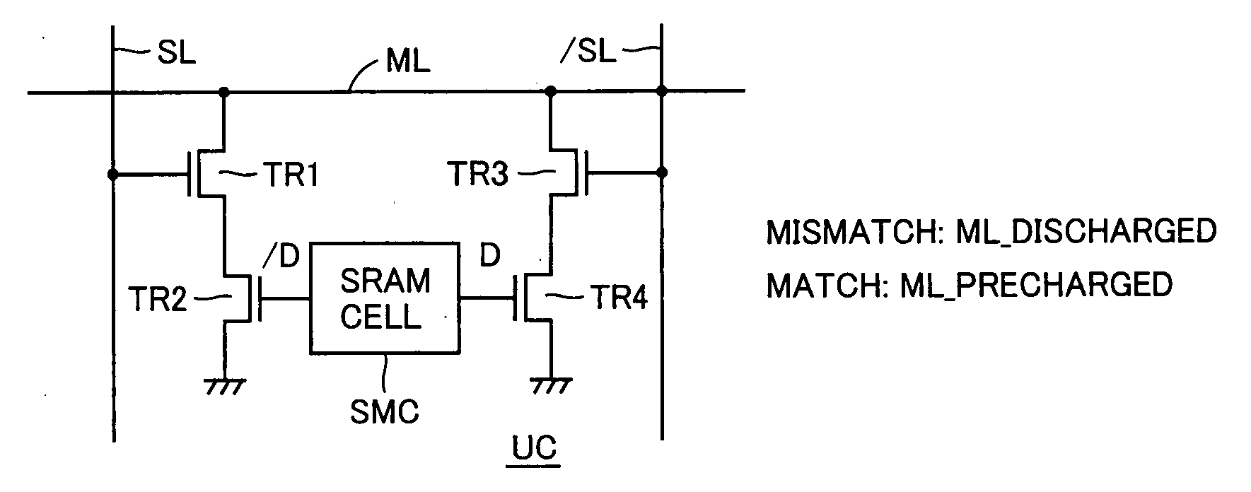
[0160]FIG. 8 shows a main portion of a content addressable memory according to a second embodiment of the invention. The content addressable memory shown in FIG. 8 differs from that shown in FIG. 4 in internal construction of latch amplifier 10. Specifically, an isolation gate circuit 30 is arranged at a preceding stage of differential amplifier circuit 12. Isolation gate circuit 30 includes isolation gates (charge confining gates) 30a and 30b that are selectively turned off according to an isolation instructing signal MLI. Isolation gate 30a selectively isolates match line ML from a positive input (+) of differential amplifier 12a. Isolation gate 30b shuts off transmission of reference voltage VREF to a negative input (−) of differential amplifier 12a. Other internal constructions shown in FIG. 8 are the same as those of the content addressable memory shown in FIG. 4. Corresponding portions are allotted the same reference numerals, and description thereof is not repeated.

[0161]FIG....

third embodiment

[0187]FIG. 11 schematically shows a whole construction a content addressable memory according to a third embodiment of the invention. Similarly to the first and second embodiments, in the content addressable memory shown in FIG. 11, memory cell array 1 is divided into a plurality of entries ERY. Match line ML is arranged for each entry ERY, and each search line pair SLP (search lines SL and / SL) is arranged for all entries ERY. The plurality of search line pairs constitute a search data bus.

[0188]Match determining circuit 2 includes match amplifiers 40 provided corresponding to respective entries ERY. Match amplifier 40 has a pull-up function of supplying a pulling-up current to a corresponding match line in the data comparing operation. A bias voltage generating circuit 45 is arranged for controlling the pull-up current supply in match amplifier 40. Match amplifier 40 supplies a pull-up current of a restricted current value to corresponding match line ML according to a bias voltage...

fourth embodiment

[0221]FIG. 16 shows a main portion of a content addressable memory according to a fourth embodiment of the invention. The content addressable memory shown in FIG. 16 differs from the content addressable memory shown in FIG. 15 in the following construction. An N-channel MOS transistor 60 is arranged corresponding to each of match lines ML (ML[0]-ML[n]) for discharging the corresponding match line to the ground voltage level in response to a discharge instructing signal DIS. Other constructions of the content addressable memory shown in FIG. 16 are the same as those of the content addressable memory shown in FIG. 15. Corresponding portions bear the same reference numbers, and description thereof is not repeated.

[0222]FIG. 17 is a timing chart representing a search operation of the content addressable memory shown in FIG. 16. Referring to FIG. 17, the operation of the content addressable memory shown in FIG. 16 will now be described.

[0223]At time T1, the search cycle starts. When the ...


PUM


Abstract

An entry including multiple bits of unit cells each storing data bit is coupled to a match line. The match line is supplied with a charging current having a restricted current value smaller than a match line current flowing in a one-bit miss state in one entry, but larger than a match line current flowing in an all-bit match state in one entry. A precharge voltage level of a match line is restricted to a voltage level of half a power supply voltage or smaller. Power consumption in a search cycle of a content addressable memory can be reduced, and a search operation speed can be increased.

Description

BACKGROUND OF THE INVENTION[0001]1. Field of the Invention[0002]The present invention relates to a content addressable memory, and particularly to a construction for reducing current consumption and a peak current in a search operation and for speeding up the search operation.[0003]2. Description of the Background Art[0004]A CAM (Content Addressable Memory) has, in addition to a function of reading / writing data, a function of determining matching of stored data with supplied search data. One entry storing a search data word is configured by a plurality of CAM cells, and stores word bits of a search candidate. Each entry is provided with a match line coupled to corresponding CAM cells in parallel. When a search data word matches a stored data word, a corresponding match line is kept at a state of “1”. When mismatch occurs, the corresponding match line is driven to a state of “0”.[0005]By determining the voltage level of the match line, it is possible to determine whether the data cor...

Claims


Application Information

Patent Timeline
IPC IPC(8): G11C15/00
CPCG11C15/04G11C15/046G11C7/12G11C7/06G11C7/14G11C7/22G11C15/043
Inventor WATANABE, NAOYAHAYASHI, ISAMUAMANO, TERUHIKOMORISHITA, FUKASHIYOSHINAGA, KENJIAKIYAMA, MIHOKOMIYAZAKI, SHINYAISHIBASHI, MASAKAZUDOSAKA, KATSUMI
Owner RENESAS TECH CORP
Why Eureka
Try Eureka