METHOD FOR GROWTH OF SEMIPOLAR (Al,In,Ga,B)N OPTOELECTRONIC DEVICES

Active Publication Date: 2007-11-01
RGT UNIV OF CALIFORNIA
View PDF30 Cites 296 Cited by
  • Summary
  • Abstract
  • Description
  • Claims
  • Application Information

AI Technical Summary

Benefits of technology

[0049] The depositing step may result in a final surface which is substantially planar. The method of the present invention may be used to fabricate a substrate or a device, for example a substrate, li

Problems solved by technology

However, conventional c-plane quantum well structures in III-nitride based optoelectronic and electronic devices suffer from the undesirable quantum-confined Stark effect (QCSE), due to the existence of strong piezoelectric and spontaneous polarizations.
The strong built-in electric fields along the c-direction cause spatial separation of electrons and holes that in turn give rise to restricted carrier recombination efficiency, reduced oscillator strength, and red-shifted emission.
Unfortunately, despite advances made by researchers at the University of California, Santa Barbara, growth of nonpolar nitrides remains challenging and has not yet been widely adopted in the III-nitride industry.
Although the Nishizuka method provided high crystal quality semipolar orientation facets, it resulted in the formation of multiple crystal

Method used


Image

  • METHOD FOR GROWTH OF SEMIPOLAR (Al,In,Ga,B)N OPTOELECTRONIC DEVICES
  • METHOD FOR GROWTH OF SEMIPOLAR (Al,In,Ga,B)N OPTOELECTRONIC DEVICES
  • METHOD FOR GROWTH OF SEMIPOLAR (Al,In,Ga,B)N OPTOELECTRONIC DEVICES

Examples


Example

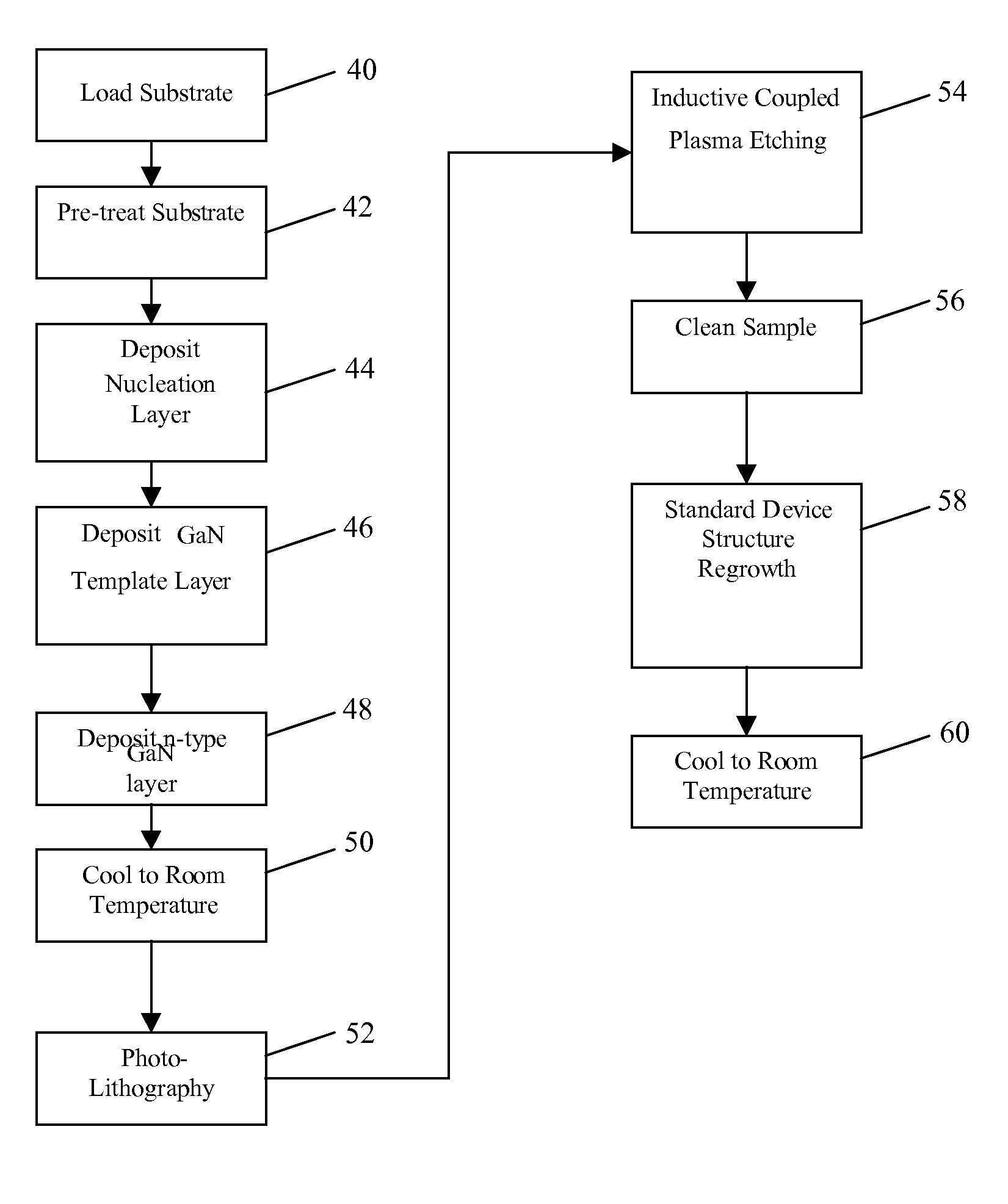
[0070] In the following description of the preferred embodiment, reference is made to the accompanying drawings which form a part hereof, and in which is shown by way of illustration a specific embodiment in which the invention may be practiced. It is to be understood that other embodiments may be utilized and structural changes may be made without departing from the scope of the present invention.

[0071] Overview

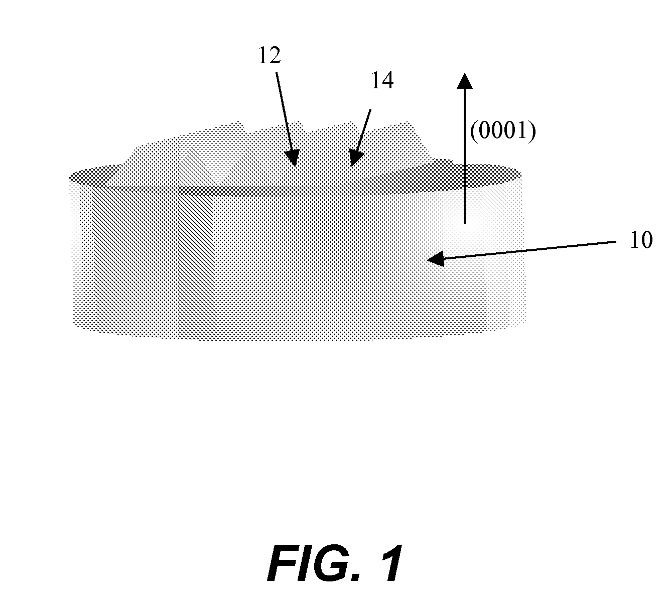
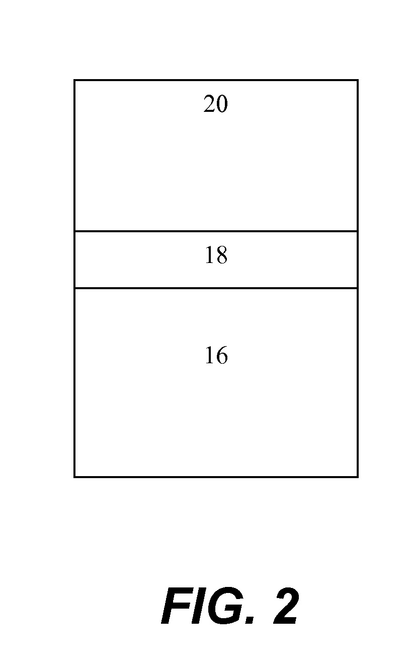
[0072] The present invention describes a novel method for growing high-efficiency (Al,In,Ga)N based optoelectronic devices wherein one or more layers of the device structure, including but not limited to the active region(s), may be described as having a semipolar orientation. The method utilizes device-quality nitride semiconductor thin film template layers, including, but not limited to c-plane GaN, grown on a c- or a-plane sapphire substrate. These layers, and subsequent device layers may be grown via techniques, including but not limited to MOCVD, MBE or HVPE. The use ...


PUM


Abstract

A method of fabricating an optoelectronic device, comprising growing an active layer of the device on an oblique surface of a suitable material, wherein the oblique surface comprises a facetted surface. The present invention also discloses a method of fabricating the facetted surfaces. One fabrication process comprises growing an epitaxial layer on a suitable material, etching the epitaxial layer through a mask to form the facets having a specific crystal orientation, and depositing one or more active layers on the facets. Another method comprises growing a layer of material using a lateral overgrowth technique to produce a facetted surface, and depositing one or more active layers on the facetted surfaces. The facetted surfaces are typically semipolar planes.

Description

CROSS-REFERENCE TO RELATED APPLICATIONS [0001] This application claims the benefit under 35 U.S.C. Section 119(e) of the following co-pending and commonly-assigned U.S. patent application: [0002] U.S. Provisional Patent Application Ser. No. 60 / 774,467, filed on Feb. 17, 2006, by Hong Zhong, John F. Kaeding, Rajat Sharma, James S. Speck, Steven P. DenBaars and Shuji Nakamura, entitled “METHOD FOR GROWTH OF SEMIPOLAR (Al,In,Ga,B) N OPTOELECTRONICS DEVICES,” attorneys docket number 30794.173-US-P1 (2006-422); [0003] which application is incorporated by reference herein. [0004] This application is related to the following co-pending and commonly-assigned applications: [0005] U.S. Utility patent application Ser. No. 11 / 054,271, filed Feb. 9, 2005, by Rajat Sharma, Paul M. Pattison, John F. Kaeding, and Shuji Nakamura, entitled “SEMICONDUCTOR LIGHT-EMITTING DEVICE,” attorneys docket number 30794.112-US-01 (2004-208); [0006] U.S. Utility patent application Ser. No. 11 / 372,914 filed Mar. 10...

Claims


Application Information

Patent Timeline
IPC IPC(8): H01L33/00H01L21/00H01L29/06
CPCH01L21/02389H01L21/0242H01L21/02458H01L21/02647H01L21/02658H01L29/2003C30B29/403H01L31/0236H01L31/18H01L33/0075Y02E10/50C30B25/186H01L29/778H01L33/16
Inventor ZHONG, HONGKAEDING, JOHN F.SHARMA, RAJATSPECK, JAMES S.DENBAARS, STEVEN P.NAKAMURA, SHUJI
Owner RGT UNIV OF CALIFORNIA
Why Eureka
Try Eureka