
Compounds for electronic devices

Active Publication Date: 2015-05-19
MERCK PATENT GMBH
View PDF61 Cites 1 Cited by
  • Summary
  • Abstract
  • Description
  • Claims
  • Application Information

AI Technical Summary

Benefits of technology

The compounds described in this patent have improved properties compared to existing materials used in OLED displays. They require less voltage to operate, leading to higher power efficiency. They also result in longer lifetimes and improved power efficiency in devices containing phosphorescent emitters. The thickness of the hole-transport layer can be increased without losing power efficiency, which is important for optimal optical coupling-out efficiency. The compounds have good efficiency and lifetime as dopants in emitting layers. They are easier to process and are more suitable for mass production compared to materials without a bridging group X.

Problems solved by technology

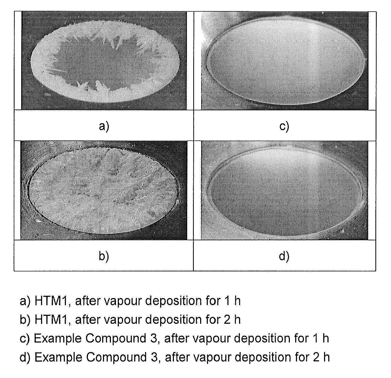
However, this cannot be achieved using materials in accordance with the prior art owing to the associated increase in voltage.5. Many materials which are used in accordance with the prior art in organic electroluminescent devices tend to crystallise on the vapour-deposition source in the process for the production of the electroluminescent device and thus clog the vapour-deposition source.
These materials can therefore only be employed in mass production with increased technical complexity.
The indenofluorenamines described above have disadvantages in processability: during the vapour-deposition or coating process, premature deposition and thus a complication of the industrial process may occur.
In addition, hole-transporting materials generally frequently have low electron stability, which results in short lifetimes of the associated diodes in operation.

Method used


Image

  • Compounds for electronic devices
  • Compounds for electronic devices
  • Compounds for electronic devices

Examples


working examples

[0101]The following syntheses are carried out, unless indicated otherwise, under a protective-gas atmosphere in dried solvents. The starting materials can be purchased from ALDRICH.

example 1

Synthesis of Example Compound 1

a) Bis[N-(2-carboxymethylphenyl)]-6,6,12,12-tetramethyl-6-12-dihydroindeno[1,2b]fluorine diamine

[0102]

35.51 g (234.9 mmol) of methyl anthranilate are dissolved in 500 ml of toluene, and the solution is thoroughly degassed. 50.0 g (106.8 mmol) of 6,6,12,12-tetramethyl-6-12-dihydroindeno[1,2b]fluorenyl dibromide, 2.1 g (10.7 mmol) of 4,5-bis(diphenylphosphino)-9,9-dimethylxanthene, 1.19 g (5.34 mmol) of Pd(OAc)2 and 76.5 g (234.9 mmol) of Cs2CO3 are added, and the mixture is subsequently degassed and stirred at 100° C. under a protective-gas atmosphere for 24 h. The solids are subsequently filtered off through Celite, and the organic phase is washed with water, dried over MgSO4 and evaporated. The crude product is washed by stirring with hot heptane, giving 56 g (86%) of the product as a yellow solid.

b) Bis[N-(2-(1-methyl-1-hydroxyethyl)phenyl)]-6,6,12,12-tetramethyl-6-12-dihydroindeno[1,2b]fluorine diamine

[0103]

56.0 g (92.0 mmol) of the compound from a)...

example compound 1

d) Example Compound 1

[0105]

50.0 g (87.3 mmol) of the bisacridine from c) and 34.75 ml (261.8 mmol) of bromobenzene are dissolved in 2500 ml of degassed toluene, and the solution is then degassed. Tri-tert-butylphosphine (6.11 ml, 1M solution in toluene) is added, 685.9 mg (3.05 mmol) of Pd(OAc)2 and 25.1 g (209.4 mmol) of sodium tert-butoxide are added, and the mixture is then briefly degassed and heated under reflux for 3 h. The reaction solution is washed with water, and the precipitated solid and the organic phase are combined, evaporated and dried azeotropically a number of times using toluene, giving 49.1 g (77%) of a yellow solid, which is purified further by means of Soxhlet extraction and crystallisation from NMP.


PUM

PropertyMeasurementUnit
Massaaaaaaaaaa
Fractionaaaaaaaaaa
Electric potential / voltageaaaaaaaaaa

Abstract

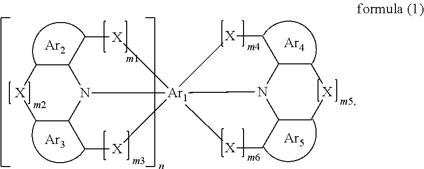
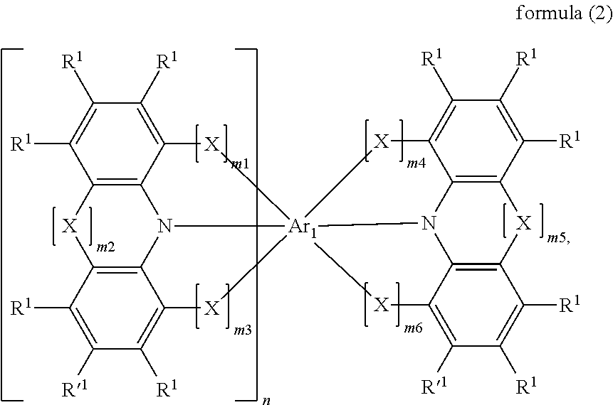
The present invention relates to compounds of the formula (1) and to the use thereof in organic electronic devices, and to organic electronic devices which comprise compounds of the formula (1), preferably as hole-transport materials and / or as emitting materials.

Description

CROSS-REFERENCE TO RELATED APPLICATIONS[0001]This application is a national stage application (under 35 U.S.C. §371) of PCT / EP2009 / 009219, filed Dec. 22, 2009, which claims benefit of German application 10 2009 005 290.9, filed Jan. 20, 2009.BACKGROUND OF THE INVENTION[0002]The present invention relates to compounds of the formula (1) and to the use thereof in electronic devices, and to electronic devices which comprise these compounds.[0003]The general structure of organic electroluminescent devices is described, for example, in U.S. Pat. Nos. 4,539,507, 5,151,629, EP 0676461 and WO 98 / 27136. However, there is still a need for improvement in these devices:[0004]1. The efficiency should still be improved, especially in the case of fluorescent OLEDs.[0005]2. The operating lifetime is still short, in particular in the case of blue emission, and consequently there is still a need for improvement here.[0006]3. The operating voltage is quite high, especially in the case of fluorescent OL...

Claims


Application Information

Patent Timeline
IPC IPC(8): H01L51/54C07D219/02C07D265/38C07D279/36C07D401/04C07D471/04C07D495/04C09B3/14C09B3/78C09B5/24C09B5/60C09B57/00H01L51/00H01L51/50
CPCC07D219/02C07D279/36C07D401/04C07D471/04C07D495/04H01L51/0059H01L51/006H01L51/0072C09B5/60C09B57/00C09B57/001C09B57/008C09B3/14C09B3/78C09B5/24C07D265/38Y10S428/917H01L51/5012H01L51/5048Y02E10/549H10K85/633H10K85/631H10K85/6572H10K50/14H10K50/11H10K50/15C09K11/06
Inventor BUESING, ARNEHEIL, HOLGERSTOESSEL, PHILIPPPARHAM, AMIR HOSSAINFORTTE, ROCCOKROEBER, JONAS VALENTIN
Owner MERCK PATENT GMBH
Learn More