Semiconductor device and manufacturing method thereof

a technology of semiconductor devices and manufacturing methods, applied in the direction of semiconductor devices, basic electric elements, electrical equipment, etc., can solve the problems of reverse breakdown voltage of the entire diode also dropping, and achieve the effect of lowering the rise voltage and lowering the breakdown voltag

Active Publication Date: 2007-11-01
NISSAN MOTOR CO LTD
View PDF6 Cites 10 Cited by
  • Summary
  • Abstract
  • Description
  • Claims
  • Application Information

AI Technical Summary

Benefits of technology

[0011] In accordance with the semiconductor device and the manufacturing method thereof according to the present invention, the hetero semiconductor region of a first conduction type that is the same as the conduction type of the semiconductor base is formed on the first main surface of the semiconductor base, the hetero semiconductor region of the second conduction type that is different from the conduction type of the semiconductor base is formed in the trenches dug on the first main surface of the semiconductor base, and both of the hetero semiconductor regions are parallelly connected to the first electrode. In such a way, the rise voltage can be lowered by the hetero semiconductor region of the first conduction type, which is parallelly connected to the first electrode, and the lowering of the breakdown voltage can be suppressed by the hetero semiconductor region of the second conduction type, which is formed in the trenches on the first main surface of the semiconductor base.

Problems solved by technology

However, in the N+ polycrystalline silicon layer, a reverse breakdown voltage thereof is also low, and accordingly, a reverse breakdown voltage of the entire diode also drops.

Method used


Image

  • Semiconductor device and manufacturing method thereof
  • Semiconductor device and manufacturing method thereof
  • Semiconductor device and manufacturing method thereof

Examples


first embodiment

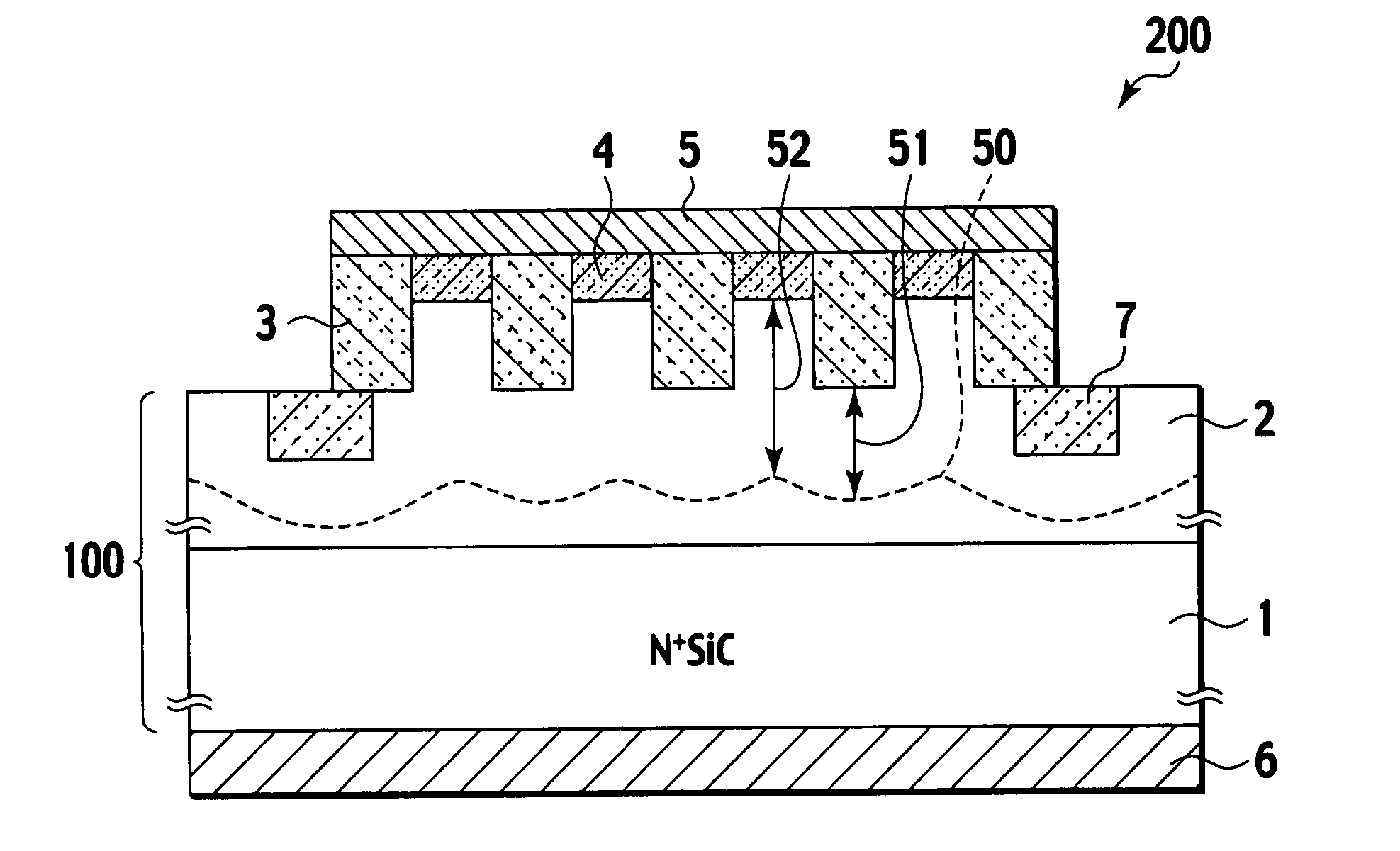
[0032] A description will be made of a first embodiment of the semiconductor device and the manufacturing method thereof according to the present invention based on FIG. 1 to FIG. 11. In this embodiment, a description will be made of, as an example, a semiconductor device, in which silicon carbide (SiC) is used as a substrate material, and polycrystalline silicon is used as a material of a hetero semiconductor. Note that, in the present invention, the substrate material is not limited to silicon carbide, and may be gallium nitride or diamond.

[0033] Moreover, the material of the hetero semiconductor is not limited to polycrystalline silicon, either, as long as the material forms a hetero semiconductor region made of a semiconductor material having a different band gap from that of a semiconductor base formed of an epitaxial layer stacked on a substrate. The hetero semiconductor may be made of monocrystalline silicon germanium, polycrystalline silicon germanium, amorphous silicon ger...

second embodiment

[0061] Next, a description will be made of a second embodiment of the semiconductor device and the manufacturing method thereof according to the present invention based on FIG. 12. FIG. 12 is a cross-sectional view showing an element portion cross-sectional structure in the second embodiment of the semiconductor device according to the present invention. In a similar way to the first embodiment, the semiconductor device 300 in this embodiment, which is shown in FIG. 12, is a device, in which silicon carbide (SiC) is used as a substrate material, and polycrystalline silicon is used as a material of a hetero semiconductor. However, as shown in FIG. 12, the semiconductor device 300 is different from the semiconductor device 200 of the first embodiment, which is shown in FIG. 1, in the connection method of the P+ polycrystalline silicon layer 3 and the anode electrode 5.

[0062] Specifically, the semiconductor device 300 of FIG. 12 is configured in the following manner. Specifically, con...

third embodiment

[0067] Next, a description will be made of a third embodiment of the semiconductor device and the manufacturing method thereof according to the present invention based on FIG. 13. FIG. 13 is a cross-sectional view showing an element portion cross-sectional view in the third embodiment of the semiconductor device according to the present invention. In a similar way to the first embodiment and the second embodiment, the semiconductor device 400 in this embodiment, which is shown in FIG. 13, is a device, in which silicon carbide (SiC) is used as a substrate material, and polycrystalline silicon is used as a material of a hetero semiconductor. However, as shown in FIG. 13, the semiconductor device 400 is different from the semiconductor devices of the first embodiment and the second embodiment in that the P+ polycrystalline silicon layer 3 and the N+ polycrystalline silicon layer 4 are formed by separately implanting the ions into the semiconductor region.

[0068] Specifically, in place ...


PUM

PropertyMeasurementUnit
temperatureaaaaaaaaaa
obtuse angleaaaaaaaaaa
angleaaaaaaaaaa

Abstract

As semiconductor regions in contact with a first main surface of a semiconductor base composed by forming an N− silicon carbide epitaxial layer on an N+ silicon carbide substrate connected to a cathode electrode, there are provided both of an N+ polycrystalline silicon layer of a same conduction type as a conduction type of the semiconductor base and a P+ polycrystalline silicon layer of a conduction type different from the conduction type of the semiconductor base. Both of the N+ polycrystalline silicon layer and the P+ polycrystalline silicon layer are hetero-joined to the semiconductor base, and are ohmically connected to the anode electrode. Moreover, the N+ polycrystalline silicon layer of the same conduction type as the conduction type of the semiconductor base is formed so as to contact the first main surface of the semiconductor base, and the P+ polycrystalline silicon layer of the conduction type different from the conduction type of the semiconductor base is formed in trenches dug on the first main surface of the semiconductor base.

Description

BACKGROUND OF THE INVENTION [0001] 1. Field of the Invention [0002] The present invention relates to a semiconductor device and a manufacturing method thereof. [0003] 2. Description of the Related Art [0004] As a conventional technology serving as a background of the present invention, there is a technology described in Japanese Patent Laid-Open Publication No. 2003-318413 “High-Breakdown-Voltage Silicon Carbide Diode and Manufacturing Method Thereof” as Patent Document 1 filed by the applicant of this invention. [0005] In the conventional technology described in Patent Document 1, on a first main surface of a semiconductor base in which an N− silicon carbide epitaxial layer is formed on an N+ silicon carbide substrate, a P+ polycrystalline silicon layer is formed, in which a band gap is different from that of the semiconductor base, and a conduction type is different from that of the semiconductor base. The N− silicon carbide epitaxial layer and the P+ polycrystalline silicon layer...

Claims


Application Information

Patent Timeline
Patent Type & Authority Applications(United States)
IPC IPC(8): H01L29/732
CPCH01L21/0465H01L21/0475H01L29/0615H01L29/8613H01L29/267H01L29/6606H01L29/66136H01L29/1608
Inventor YAMAGAMI, SHIGEHARUHOSHI, MASAKATSUSHIMOIDA, YOSHIOHAYASHI, TETSUYATANAKA, HIDEAKI
Owner NISSAN MOTOR CO LTD
Why Eureka
Try Eureka