Method for manufacturing a light-emitting device with a periodic structure in an active region

Inactive Publication Date: 2007-11-01
SUMITOMO ELECTRIC IND LTD
View PDF1 Cites 15 Cited by
  • Summary
  • Abstract
  • Description
  • Claims
  • Application Information

AI Technical Summary

Benefits of technology

[0010] The method according to the present invention may form the other grating region simultaneously with the formation of the first grating region. That is, the process for dry-etching the semiconductor layer may be carried out by using the etching mask that provides patterns for the first grating and also for the other grating, and a subsequent process for burying the active region within etched grooves in

Problems solved by technology

However, the dry-etching for the active region may induce plasma damage in the active region, which causes dislocations and defects

Method used


Image

  • Method for manufacturing a light-emitting device with a periodic structure in an active region
  • Method for manufacturing a light-emitting device with a periodic structure in an active region
  • Method for manufacturing a light-emitting device with a periodic structure in an active region

Examples


second embodiment

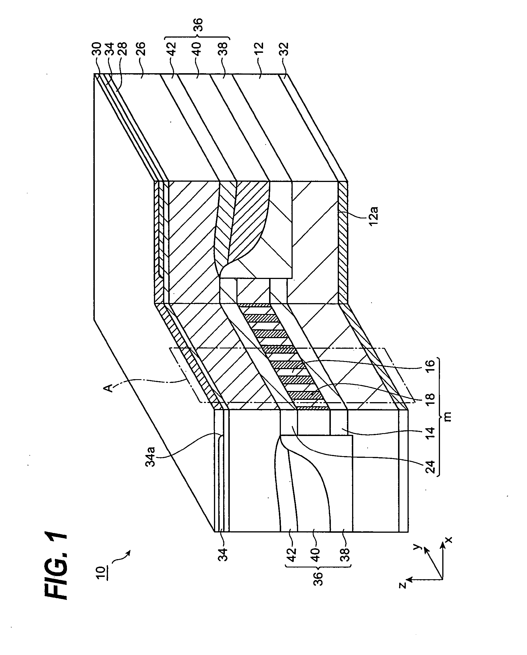
[0031] FIGS. from 3 to 7 schematically show processes for manufacturing the light-emitting device shown in FIG. 1. Next, respective processes shown in FIGS. from 3 to 7 will be described.

[0032] Growth of Group III-V Compound Semiconductor Layers)

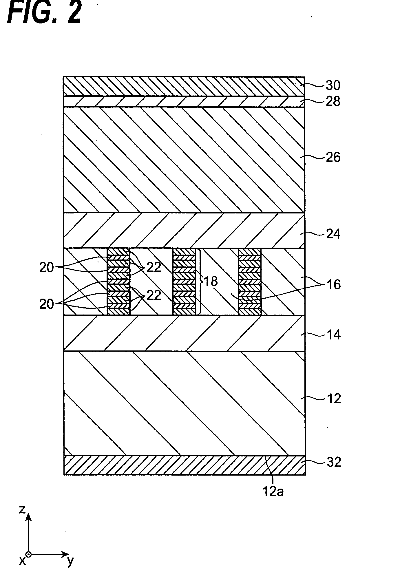
[0033] First, a group III-V compound semiconductor layer 16a is grown on the substrate 12. The substrate 12 provides with the lower cladding layer. The lower optical confinement layer 14 may be grown, if necessary, on the substrate 12 prior to the growth of the semiconductor layer 16a. The MOVPE (Metal-Organic Vapor Phase Epitaxy) method may grow the layer 16a and the lower optical confinement layer 14. The growth temperature of these layers may be 650° C.

[0034] (Forming Etching Mask)

[0035] Next, an etching mask M is formed on the semiconductor layer 16, as shown in FIG. 4. The mask M may be made of silicon oxides and patterned with the lithography technique. For instance, a stacked semiconductor layers of the substrate 12, the lower con...

third embodiment

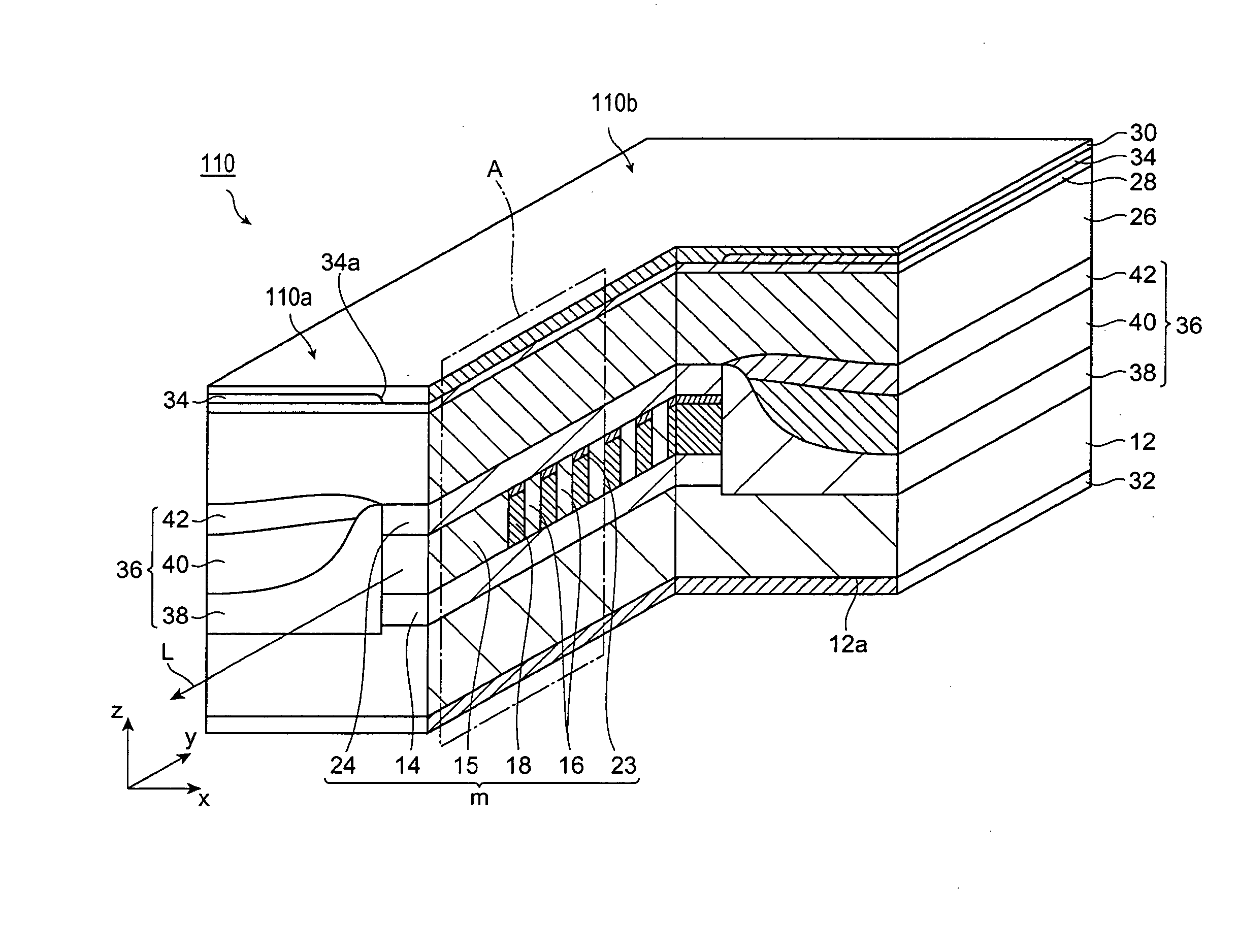
[0053] A light-emitting device according 110 to third embodiment of the invention provides an active region that includes AlGaInAs and an additional layer 23 made of group III-V compound semiconductor material between the active region 18 and the optical confinement layer 24 to prevent the oxidization of aluminum (Al) contained within the active region. The additional layer 23, involved within the mesa structure m, may be i-GaInAsP. The active region 18 may includes well layers and barrier layers each comprised of i-AlGaInAs but different compositions to each other; or the active region may include i-AlGaInAs layers for the well layer 20, while i-GaInAsP layers for the barrier layer 22. Because the device 110 provides the additional layer 23 to prevent the oxidization of the AlGaInAs layer included within the active region 18, the device may enhance the reliability as well as the performance thereof.

[0054] The light-emitting device 110 may further provide a window region 15 in an e...

fourth embodiment

[0059] Next, a fourth embodiment of the light-emitting device according to the present invention will be described. FIG. 11 is a side cross section of the light-emitting device 120 of the fourth embodiment, which is a type of distributed feedback (DFB) laser diode.

[0060] The device 120 that emits light along the y-axis includes, similar to the previous embodiments, the substrate 12 made of a group III-V compound semiconductor material, two optical confinement layers, 14 and 24, semiconductor regions 16, the active regions 18, the additional layer 23 to prevent the oxidization of the active region 18, the semiconductor layer 26 that functions as the cladding layer, the contact layer 28 and two electrodes, 30 and 32.

[0061] The device 120 also provides the window region 15 in the end portion 120a thereof from which the laser light 100L emits. On the other hand, the other end portion 120b provides a distributed Bragg reflector (DBR) 17 to reflect light 100L. The DBR 17 may omit the co...


PUM


Abstract

The invention provides a light-emitting device, where the active region thereof may be escaped from being damaged by the plasma process. The device is first formed with a semiconductor layer on the semiconductor substrate, next provided with an etching mask. Using the mask, the semiconductor layer on the substrate is dry-etched to form a periodic structure with grooves and mesas. The active regions are buried within the grooves by the OMVPE method.

Description

BACKGROUD OF THE INVENTION [0001] 1. Field of the Invention [0002] The present invention relates to a method for manufacturing a light-emitting device that provides a periodic structure along a direction to which the light is emitted. [0003] 2. Relater Prior Art [0004] A laser diode with a distributed feedback structure has been well known as a DFB laser diode. To form the distributed feedback structure, a periodic undulation is induced in an active layer by dry-etching the active layer after the planar growth thereof. A Japanese Patent Application published as JP-2004-055797A has disclosed such manufacturing process for the DFB laser diode. [0005] However, the dry-etching for the active region may induce plasma damage in the active region, which causes dislocations and defects to degrade the efficiency for emitting light due to non-radiative recombination centers brought by such imperfections in the lattice. Thus the threshold current of the laser diode increases. SUMMARY OF THE IN...

Claims


Application Information

Patent Timeline
IPC IPC(8): H01S5/00H01S3/06H01S3/14
CPCB82Y20/00H01S5/1203H01S5/1225H01S5/3412H01S5/1231H01S5/2275H01S5/341H01S5/1228
Inventor YAGI, HIDEKI
Owner SUMITOMO ELECTRIC IND LTD
Why Eureka
Try Eureka