Chip structure and fabricating process thereof

a technology of semiconductor structure and fabrication process, which is applied in the direction of semiconductor/solid-state device details, electrical apparatus, semiconductor devices, etc., can solve the problems of liquid crystal display module abnormal display, underfill material may not form a tight contact with the active surface of the driving chip, and may affect the overall yield of the chip. , to achieve the effect of increasing the overall yield of the chip

Inactive Publication Date: 2007-11-08
NOVATEK MICROELECTRONICS CORP
View PDF1 Cites 17 Cited by
  • Summary
  • Abstract
  • Description
  • Claims
  • Application Information

AI Technical Summary

Benefits of technology

[0024]In the present invention, a trap layer is formed between two adjacent bumps so that moisture or contaminants (for example, the dust particles with halogen-containing ions) attached to the chip structure can react with the trap layer between two adjacent bumps. Hence, the contamina

Problems solved by technology

However, in the process of fabricating the chip, the active surface of the driving chip may be contaminated by chemical substances or particulate impurities.
Thus, the underfill mater

Method used


Image

  • Chip structure and fabricating process thereof
  • Chip structure and fabricating process thereof
  • Chip structure and fabricating process thereof

Examples


Embodiment Construction

[0030]Reference will now be made in detail to the present preferred embodiments of the invention, examples of which are illustrated in the accompanying drawings. Wherever possible, the same reference numbers are used in the drawings and the description to refer to the same or like parts.

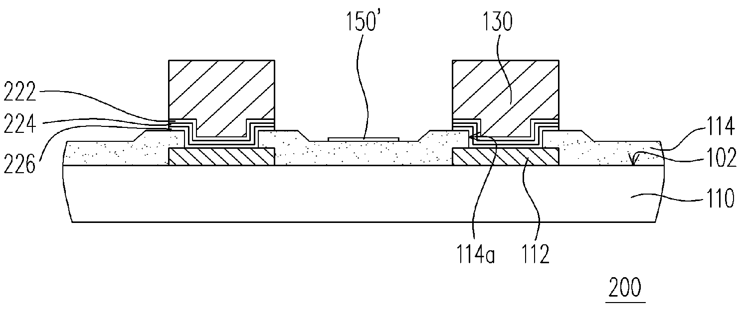
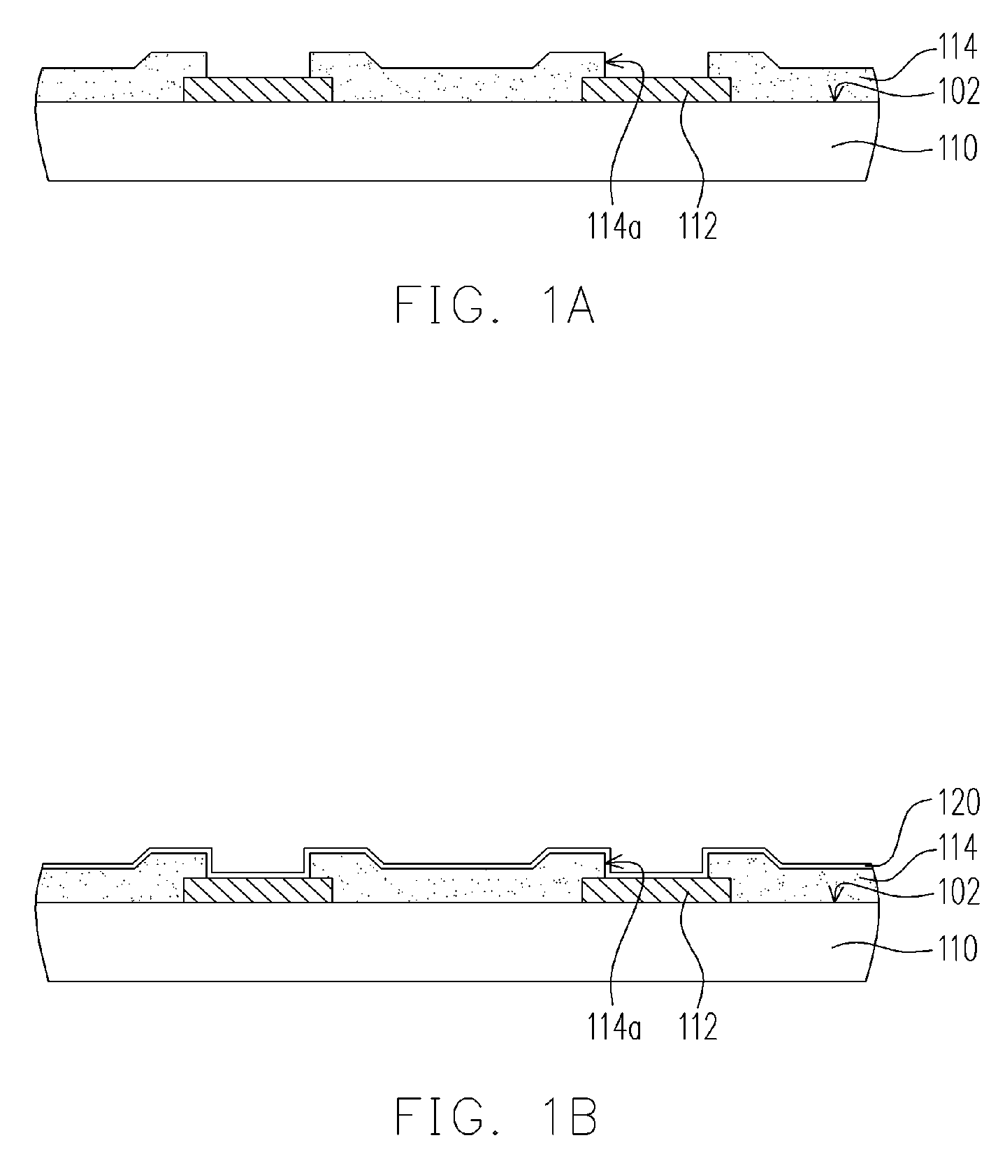
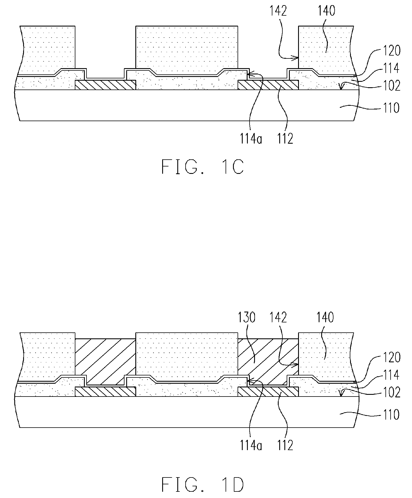
[0031]FIGS. 1A through 1H are schematic cross-sectional views showing the steps for fabricating a chip structure according to one preferred embodiment of the present invention. First, as shown in FIG. 1A, a substrate 110 is provided. The substrate 110 is, for example, a wafer or a substrate having a surface 102. Furthermore, the substrate 110 has a plurality of pads disposed on the surface 102. The material constituting the pads 112 includes, for example, aluminum. In addition, a passivation layer 114 is also formed on the surface 102 of the substrate 110 for protecting the circuit (not shown) in the outermost layer of the substrate 110. The passivation layer 114 may have a plurality of openings 114a...


PUM


Abstract

A chip structure comprising a substrate, a conductive layer, a plurality of bumps and a trap layer is provided. The substrate has a plurality of pads and the conductive layer is disposed on the pads. The bumps are disposed on the conductive layer above the pads and the trap layer is disposed between two adjacent bumps. In addition, a process of fabricating the chip structure is provided.

Description

CROSS-REFERENCE TO RELATED APPLICATION[0001]This application claims the priority benefit of Taiwan application serial no. 95115552, filed on May 2, 2006. All disclosure of the Taiwan application is incorporated herein by reference.BACKGROUND OF THE INVENTION[0002]1. Field of the Invention[0003]The present invention relates to a semiconductor structure and fabricating process thereof, and more particularly, to a chip structure and fabricating process thereof.[0004]2. Description of Related Art[0005]In general, flexible carrier packaging techniques, including the tape automated bonding (TAB) technique and chip-on-film (COF) bonding technique, are used in many different types of applications. Using the process of joining a liquid crystal display panel with a driving chip as an example, the method includes first providing a flexible substrate; the flexible substrate has a surface with a circuit layer, and the circuit layer has a plurality of inner leads. Then, a driving chip is provided...

Claims


Application Information

Patent Timeline
IPC IPC(8): H01L23/20
CPCH01L23/26H01L23/564H01L24/11H01L2224/1147H01L2224/13099H01L2924/01033H01L2924/01022H01L2924/01074H01L2924/01079H01L2924/01082H01L2924/01013H01L24/03H01L24/05H01L24/13H01L2224/05001H01L2224/05022H01L2224/05027H01L2224/0508H01L2224/05124H01L2224/05572H01L2224/05644H01L2224/10122H01L2924/00014
Inventor CHANG, HUI-LING
Owner NOVATEK MICROELECTRONICS CORP
Why Eureka
Try Eureka