

GaN crystal substrate and method of manufacturing the same, and method of manufacturing semiconductor device
- Summary
- Abstract
- Description
- Claims
- Application Information
AI Technical Summary
Benefits of technology
Problems solved by technology
Method used
Image

Examples
first embodiment
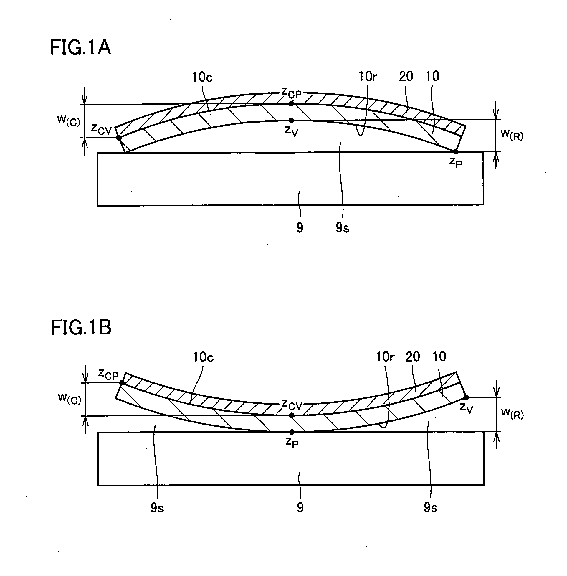
[0026] Referring to FIGS. 1A and 1B, in an embodiment of a GaN crystal substrate in accordance with the present invention, a rear surface 10r opposite to a crystal growth surface 10c has a warpage w(R) satisfying −50 μm≦w(R)≦50 μm, where a warpage causing rear surface 10r to be concavely curved as shown in FIG. 1A is indicated with a positive (+) sign, and a warpage causing rear surface 10r to be convexly curved as shown in FIG. 1B is indicated with a negative (−) sign. Warpage w(R) is defined as a difference in height between a displacement value zP at the most convex portion and a displacement value zV at the most concave portion of rear surface 10r.
[0027] Referring to FIGS. 1A and 1B, if warpage w(R) of rear surface 10r satisfies w(R)(R)>50 μm, a gap portion 9s formed between a GaN crystal substrate 10 and a susceptor 9 is increased. This results in uneven distribution of heat transferred from susceptor 9 to GaN crystal substrate 10 when at least one group-III nitride crystal la...
second embodiment
[0060] Referring to FIG. 8, a method of manufacturing a GaN crystal substrate in accordance with the present invention is a method of manufacturing the GaN crystal substrate in the first embodiment, including the steps of cutting GaN crystal substrate 10 out of a GaN crystal 1 (see FIG. 8(a)) and processing rear surface 10r of GaN crystal substrate 10 (see FIG. 8(b)), and the step of processing rear surface 10r of GaN crystal substrate 10 includes at least one of the steps of grinding rear surface 10r, lapping rear surface 10r, and etching rear surface 10r.
[0061] Referring to FIG. 8(a), the step of cutting GaN crystal substrate 10 out of GaN crystal 1 is the step of cutting GaN crystal substrate 10 of a predetermined shape out of grown GaN crystal 1 using an inner diameter blade, an outer diameter blade, a wire saw, or the like. Although there is no particular limitation on the method of growing GaN crystal 1, vapor phase epitaxy such as HVPE or MOVPE is preferably used because a l...
third embodiment
[0070] Referring to FIG. 9, an embodiment of a method of manufacturing a semiconductor device in accordance with the present invention includes the step of preparing GaN crystal substrate 10 in the first embodiment as a substrate and growing at least one group-III nitride crystal layer 20 on the side of crystal growth surface 10c of GaN crystal substrate 10. With such a manufacturing method, group-III nitride crystal layer 20 can be formed evenly and stably as a semiconductor layer on the side of crystal growth surface 10c of GaN crystal substrate 10, and thus a semiconductor device 99 having excellent properties can be obtained.
[0071] More specifically, referring to FIG. 9(a), in the method of manufacturing the semiconductor device in the present embodiment, an n-type GaN layer 21, an In0.2Ga0.8N layer 22, an Al0.2Ga0.5N layer 23, and a p-type GaN layer 24 are formed in order as group-III nitride crystal layer 20 on crystal growth surface 10c of GaN crystal substrate 10 to obtain ...
PUM
 Abstract
Description
Claims
Application Information