Power semiconductor module

a technology of power semiconductor modules and semiconductor modules, applied in the direction of printed circuit aspects, stress/warp reduction of printed circuits, and the improvement of metal adhesion of the insulation substrate, can solve the problems of power semiconductor modules experiencing critical failures, solder and other materials themselves having insufficient heat resistance, and conventional mounting structures cannot be applied to high-temperature operation that exceeds 200° c. , to achieve the effect of reducing the volume of heat sinks

Inactive Publication Date: 2007-11-15
HONDA MOTOR CO LTD
View PDF3 Cites 50 Cited by
  • Summary
  • Abstract
  • Description
  • Claims
  • Application Information

AI Technical Summary

Benefits of technology

[0039]When a SiC semiconductor power device is mounted, the system can operate at temperatures in excess of 200° C., at which best use is made of the high-temperature operating characteristics of SiC. When the structure according to the present invention is applied to a silicon device, a power semiconductor module can be achieved that has higher reliability and that can operate at a higher temperature than conventional devices.
[0040]Second, since a temperatur

Problems solved by technology

However, a conventional mounting structure cannot be applied to high-temperature operation that exceeds 200° C., which is the temperature range at which best use is made of the characteristics of a SiC semiconductor power device.
Assuming that a power semiconductor module obtained using a conventional mounting technique is employed or stored in a high-temperature environment that exceeds 200° C., or in an environment with considerable variation in the minimum and maximum temperatures, the power semiconductor module will experience a critical failure because heat stress caused by the difference in the coefficients of thermal expansion between the constituent materials becomes excessively high, and the solder and other materials the

Method used


Image

  • Power semiconductor module
  • Power semiconductor module
  • Power semiconductor module

Examples


first embodiment

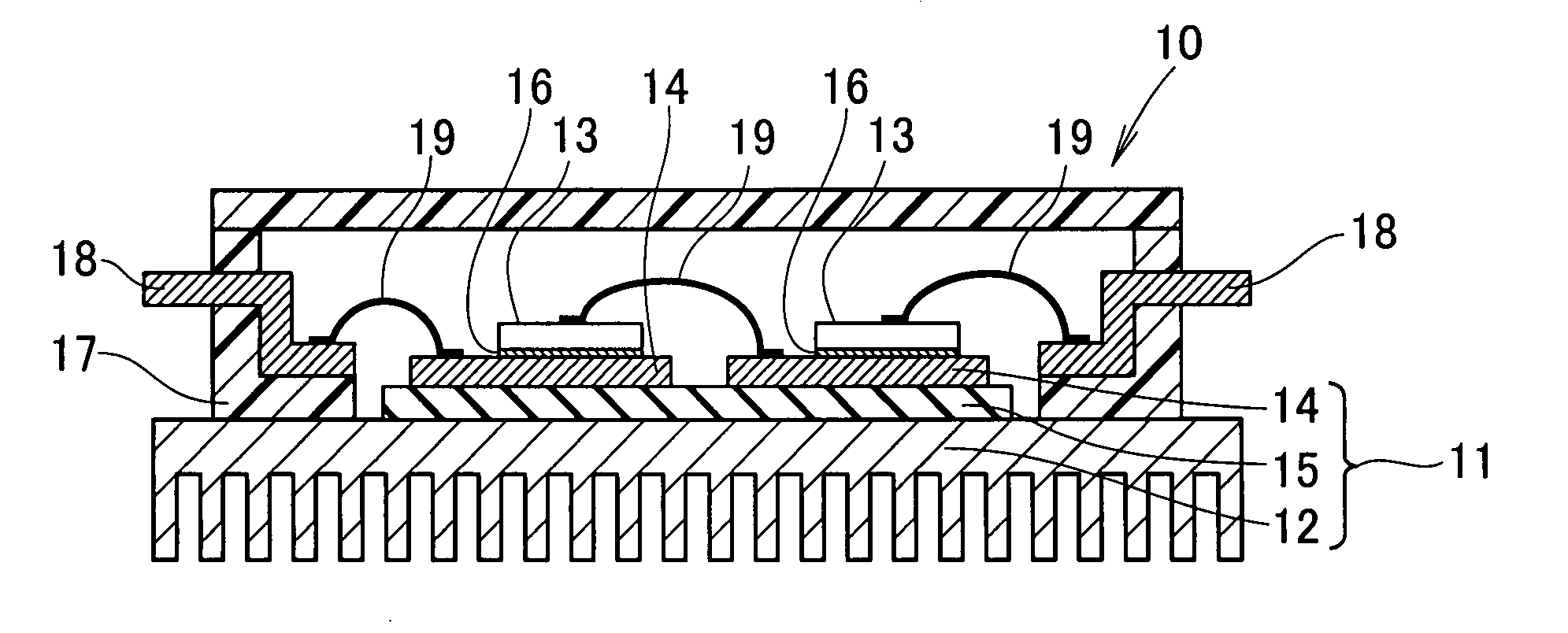
[0058]In the power semiconductor module 10 loss can be reduced by half or more in the mounted SiC semiconductor power devices 13 in comparison with a conventional silicon semiconductor power device, and since higher temperature operation is made possible, the temperature difference between the outside air and the heat sink 12 can be doubled or more greatly increased. The size (volume) of the heat sink 12 can thereby be considerably reduced to about ⅕ the size of that in a conventional module.

[0059]Based on the above, the power semiconductor module 10 according to the first embodiment is a modular structure having the following three characteristics.

[0060]First, the circuit board 11 has a simple and multi-functional structure in which the metal substrate electrodes 14, insulation substrate 15, and heat sink 12 are integrated.

[0061]Second, since the heat stress produced in the circuit board 11 is very low, the mounted SiC semiconductor power devices 13 can operate at temperatures in ...
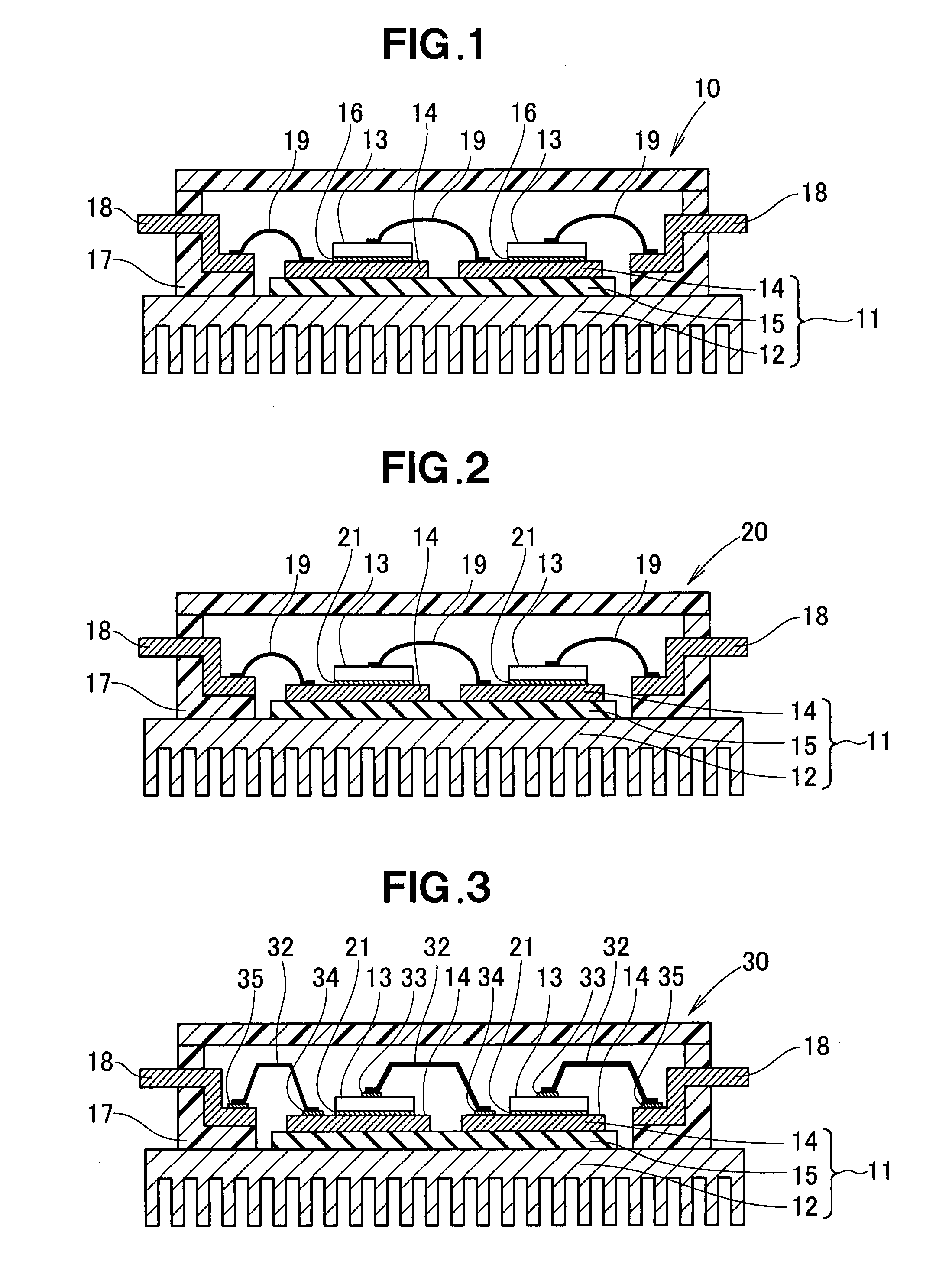
second embodiment

[0072]In the second embodiment, high ambient temperature resistance can be achieved even when AuSn solder 21 is used. This is because of the small difference in the average coefficients of thermal expansion between the SiC semiconductor power devices 13 and the metal substrate electrodes 14 of the integral circuit board 11. The difference is 3 ppm / ° C. or less at about 300° C., which is the joining temperature of AuSn 21 solder.

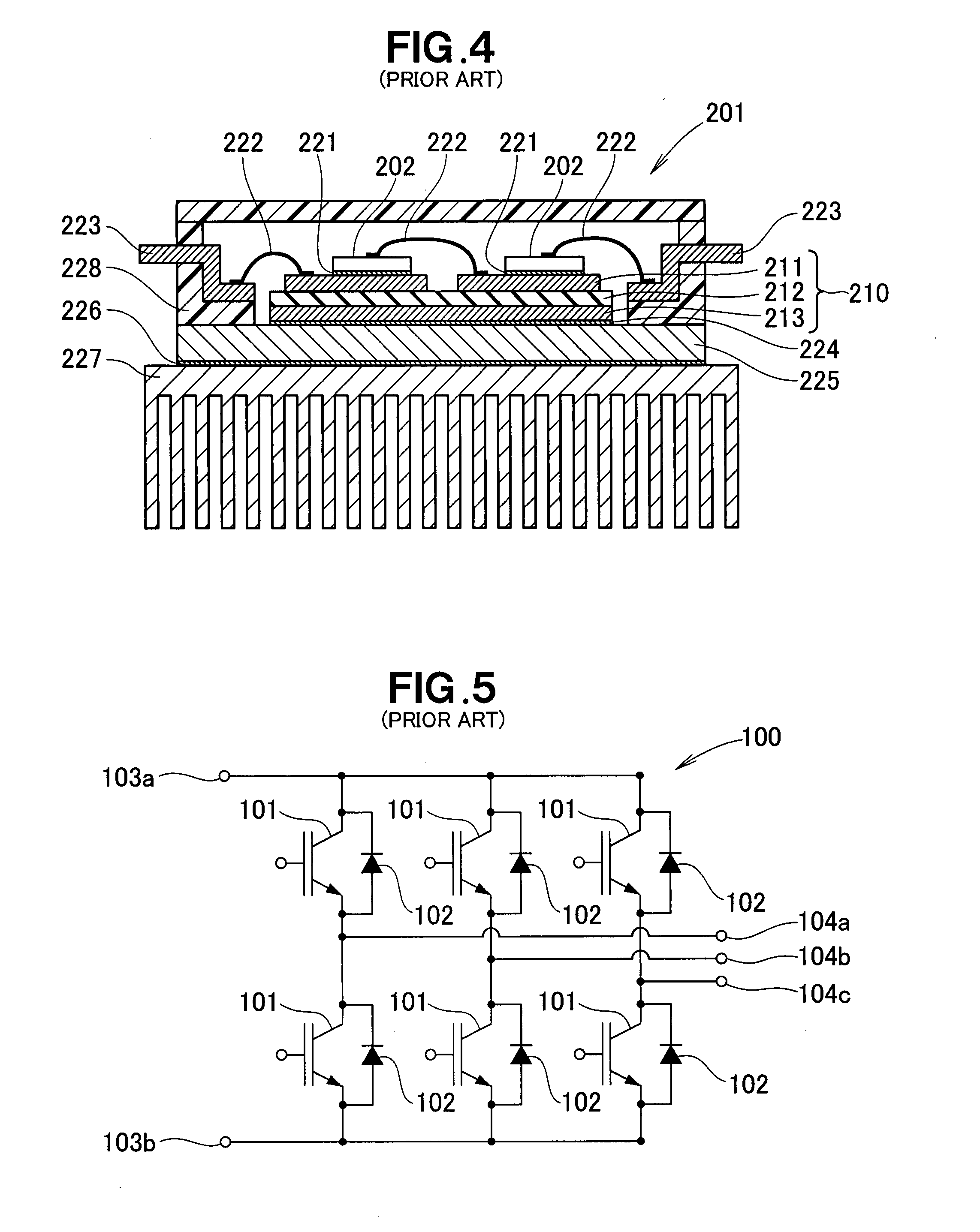
[0073]TABLE 2 below shows the results of joining SiC semiconductor power devices to two different types of circuit board structures by using AuSn solder, and performing a temperature cycle test in a temperature range of −40° C. to 200° C. Abnormalities were observed early in the test in the conventional structure, i.e., Al / AlN / Al, but abnormalities were not observed at 10,000 cycles in the structure of the present embodiment, i.e., Mo / AlN / CuC.

TABLE 2Temperature cycle test results for AuSnStructureResultsMo / AlN / CuC10,000 cycles with no abnormalitiesAl / AlN / AlCh...


PUM


Abstract

A power semiconductor module having an integral circuit board with a metal substrate electrode, an insulation substrate and a heat sink joined is disclosed. A SiC semiconductor power device is joined to a top of the metal substrate electrode of the circuit board. A difference in average coefficients of thermal expansion between constituent materials of the circuit board in a temperature range from room to joining time temperatures is 2.0 ppm/° C. or less, and a difference in expansion, produced by a difference between a lowest operating temperature and a joining temperature, of the circuit-board constituent materials is 2,000 ppm or less.

Description

FIELD OF THE INVENTION[0001]The present invention relates to a power semiconductor module and, more particularly, to a power semiconductor module that may be suitably used as a power conversion device on an automobile or the like.BACKGROUND OF THE INVENTION[0002]Semiconductor power devices are used as inverters, DC / DC converters, and other power conversion devices. Semiconductor power devices are primarily used in the form referred to as “power semiconductor modules” in which a plurality of semi-conductor power devices is mounted.[0003]The structure of a typical conventional power semi-conductor module is described below with reference to FIGS. 4 and 5 hereof. FIG. 4 shows a cross-sectional structure of the power semiconductor module, while FIG. 5 shows an electric circuit built into the power semiconductor module.[0004]Examples of such semiconductor power devices include transistors in which ON / OFF operation is controlled by an external signal, diodes having rectifying characterist...

Claims


Application Information

Patent Timeline
IPC IPC(8): H01L23/62
CPCH01L23/057H01L2224/32225H01L25/072H01L2224/48091H01L2224/48472H01L2924/01079H01L2924/13055H01L2924/13091H01L2924/14H01L2924/16195H01L2924/19107H01L2924/3011H05K1/0271H05K1/0306H05K3/0061H05K3/38H05K2201/0355H05K2201/068H01L23/3735H01L2924/1305H01L24/48H01L2224/45124H01L2224/48227H01L2224/73265H01L2924/00014H01L2924/00H01L24/45H01L2924/00015H01L25/07H01L25/18H01L23/373
Inventor NONAKA, KENICHIKATO, TAKESHIOOGUSHI, KENJIHIGASHIDANI, YOSHIHIKOSAITO, YOSHIMITSUOKAMOTO, KENJI
Owner HONDA MOTOR CO LTD
Why Eureka
Try Eureka