Semiconductor memory device

a technology of memory devices and semiconductors, applied in semiconductor devices, digital storage, instruments, etc., can solve the problems of degrading reaching the scaling limitation, etc., and achieve the effect of retaining the retaining capacity of stored data in data readou

Active Publication Date: 2007-11-15
RENESAS ELECTRONICS CORP
View PDF3 Cites 131 Cited by
  • Summary
  • Abstract
  • Description
  • Claims
  • Application Information

AI Technical Summary

Benefits of technology

[0008]In view of the foregoing, an object of the present invention is to provide a semico

Problems solved by technology

Although the DRAM (Dynamic Random Access Memory) formed of stacked type or trench type memory capacitors and transistors for switching assumes a dominant position in the field of semiconductor memory devices of high density, it is now reaching the scaling limitation

Method used


Image

  • Semiconductor memory device
  • Semiconductor memory device
  • Semiconductor memory device

Examples


first embodiment

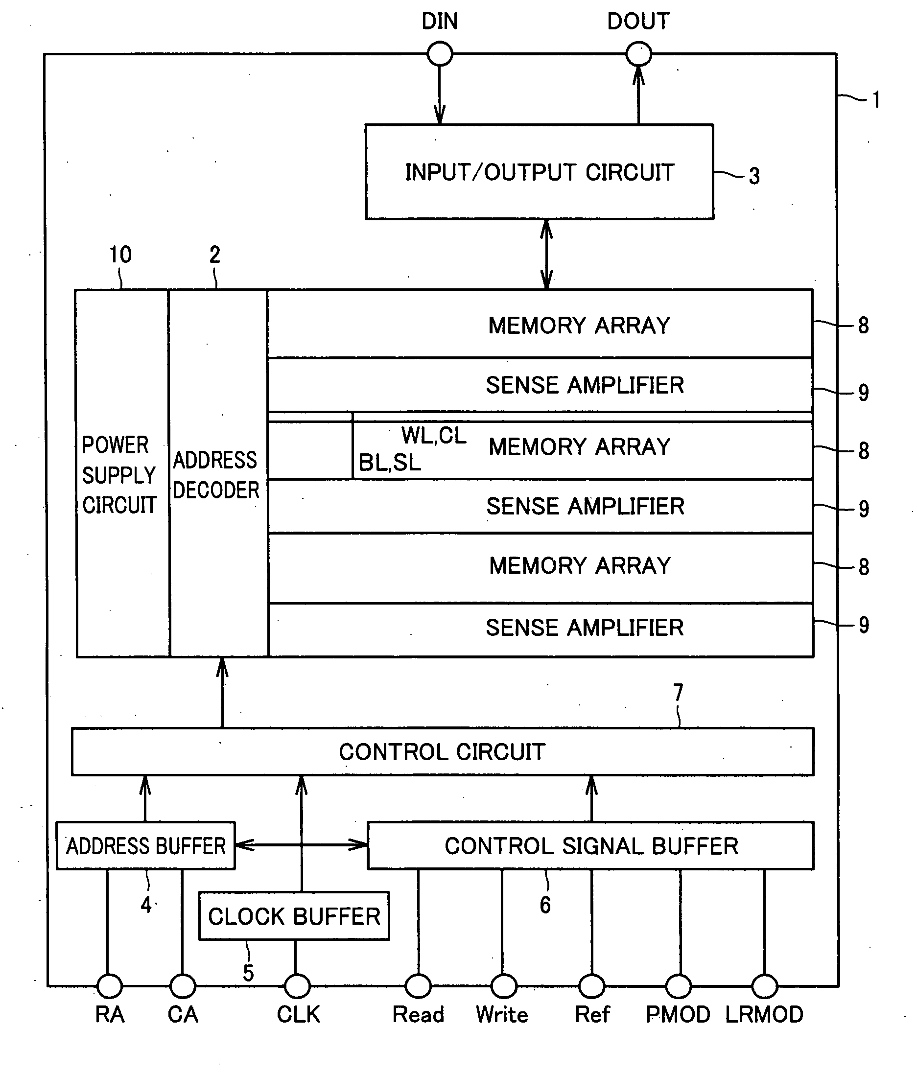
[0028]Referring to FIG. 1, a semiconductor memory device 1 according to a first embodiment of the present invention includes an address decoder 2, an input / output circuit 3, an address buffer 4, a clock buffer 5, a control signal buffer 6, a control circuit 7, a memory array 8, a sense amplifier 9, and a power supply circuit 10.

[0029]Address decoder 2 is configured including a row address decoder (not shown) and a column address decoder (not shown). Address decoder 2 responds to a control command, based on a row address signal RA and a column address signal CA applied to a terminal of semiconductor memory device 1 from an external source, to selectively drive a plurality of word lines WL and charge lines CL arranged along the row direction of memory array 8, as well as a plurality of bit lines BL and source lines SL arranged along the column direction of memory array 8.

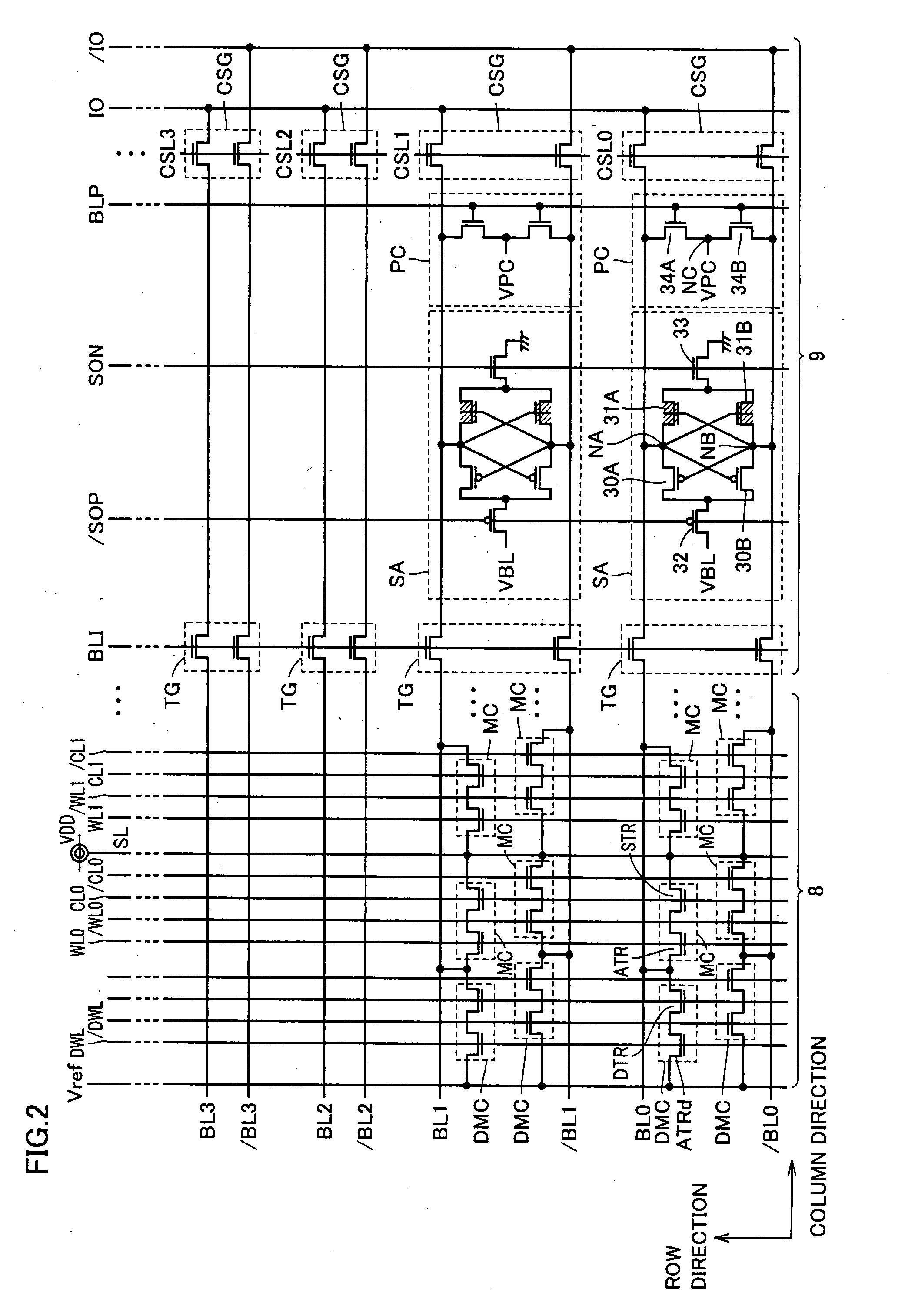
[0030]Sense amplifier 9 includes a sense amplifier circuit corresponding to each bit line pair. Two bit lines BL ad...

second embodiment

[0134]The schematic diagram of a semiconductor memory device according to a second embodiment of the present invention is similar to that of the semiconductor memory device of the first embodiment shown in FIGS. 1 and 2. Therefore, detailed description thereof will not be repeated. In the second embodiment of the present invention, the circuit configuration of the sense amplifier is arbitrary. A circuit configuration other than that of sense amplifier 9 shown in FIG. 2 may be employed. In the second embodiment of the present invention, channel formation region 23 corresponds to “channel formation region”. Impurity diffusion region 24 and impurity diffusion region 22 correspond to “first impurity diffusion region” and “second impurity diffusion region”, respectively.

[0135]The second embodiment of the present invention will be described based on a data retaining operation in a state where data “0” is stored in memory cell MC. i.e. the amount of accumulated holes at storage node SN is ...


PUM


Abstract

When data “1” is stored in a memory cell, a bit line is driven to an H level (control line drive potential) and the other bit line is driven to an L level (reference potential) when a sense operation is completed. When a verify write operation is initiated, a charge line is driven from an H level (power supply potential) to an L level (reference potential). By the GIDL current from a source line, accumulation of holes is initiated again for a storage node subsequent to discharge of holes, whereby the potential of the storage node rises towards an H level (period α). When the charge line is driven to an H level from an L level, the potential of the storage node further rises (period β).

Description

BACKGROUND OF THE INVENTION[0001]1. Field of the Invention[0002]The present invention relates to random access semiconductor memory devices, and more particularly to the technique of employing a memory cell that is formed including a transistor with a storage node.[0003]2. Description of the Background Art[0004]Although the DRAM (Dynamic Random Access Memory) formed of stacked type or trench type memory capacitors and transistors for switching assumes a dominant position in the field of semiconductor memory devices of high density, it is now reaching the scaling limitation due to the difficulty in microminiaturization of the memory capacitor. Under such circumstances, there is proposed a memory cell that employs the transistor per se as the capacitor element as an alternative to the configuration that includes a memory capacitor such as the DRAM.[0005]Among such new type of memory cells, there is known a promising twin transistor RAM (TTRAM: Twin Transistor Random Access Memory). Fo...

Claims


Application Information

Patent Timeline
IPC IPC(8): G11C7/02
CPCG11C7/065H01L29/7841G11C7/1048G11C7/14G11C11/405G11C11/4091G11C11/4099G11C2207/002G11C2207/005G11C2207/2281H01L21/84H01L27/10802H01L27/10844H01L27/10897H01L27/1203G11C7/08H10B12/20H10B12/01H10B12/50
Inventor MORISHITA, FUKASHIARIMOTO, KAZUTAMI
Owner RENESAS ELECTRONICS CORP
Why Eureka
Try Eureka