Optical receiving device
a technology of optical receiving device and optical receiver, which is applied in the direction of semiconductor devices, diodes, electrical apparatus, etc., can solve the problems of reducing the response speed, increasing the traveling distance of carriers, and reducing the sensitivity of silicon optical receiving devi
- Summary
- Abstract
- Description
- Claims
- Application Information
AI Technical Summary
Benefits of technology
Problems solved by technology
Method used
Image
Examples
first embodiment
[0087]A silicon optical receiving device of the lateral type, which is constructed as shown in FIG. 8B, will be described. A PF doped FT-Si photocarrier generation layer is formed by using silicon as the matrix semiconductor, the P atom as an n-type dopant D substituted for a lattice site, and the F atom as a heteroatom Z inserted into an interstitial site. The PF pair concentration is set to 5×10²¹ / cm3. The concentrations of the P atoms and the F atoms are determined by secondary ion mass spectroscopy (SIMS).
[0088]To determine whether a PF pair of a pendant type FT structure is formed in the photocarrier generation layer 13, it is effective to examine the vibration mode inherent in the PF pair, which can be detected by microspectroscopy of the photocarrier generation layer. A method for easily checking the PF pair formation is to form a PF-doped region having the same composition as that of the photocarrier generation layer and a region doped only with P on the surface of a high-re...
second embodiment
[0097]An optical receiving device having exactly the same configuration as that in the first embodiment is produced except that the B atom, a p-type dopant, is used as the dopant D and the K atom is used as the heteroatom Z. The B concentration and K concentration as determined by SIMS are both 4×10²¹ / cm3, and the BK pair concentration is estimated at 4×10²¹ / cm3.
[0098]To determine whether a BK pair of the pendant type FT structure is formed in the photocarrier generation layer, it is effective to determine the vibration mode inherent in the BK pair. It can also be determined by using a simpler method based of the resistivity value or carrier concentration.
[0099]FIG. 11 shows the response characteristics of output light currents observed when optical signals with a wavelength of 850 nm modulated at 10 GHz are input to the optical receiving device according to the embodiment. As is apparent from FIG. 11, output light currents having the same waveform are obtained in response to the in...
third embodiment
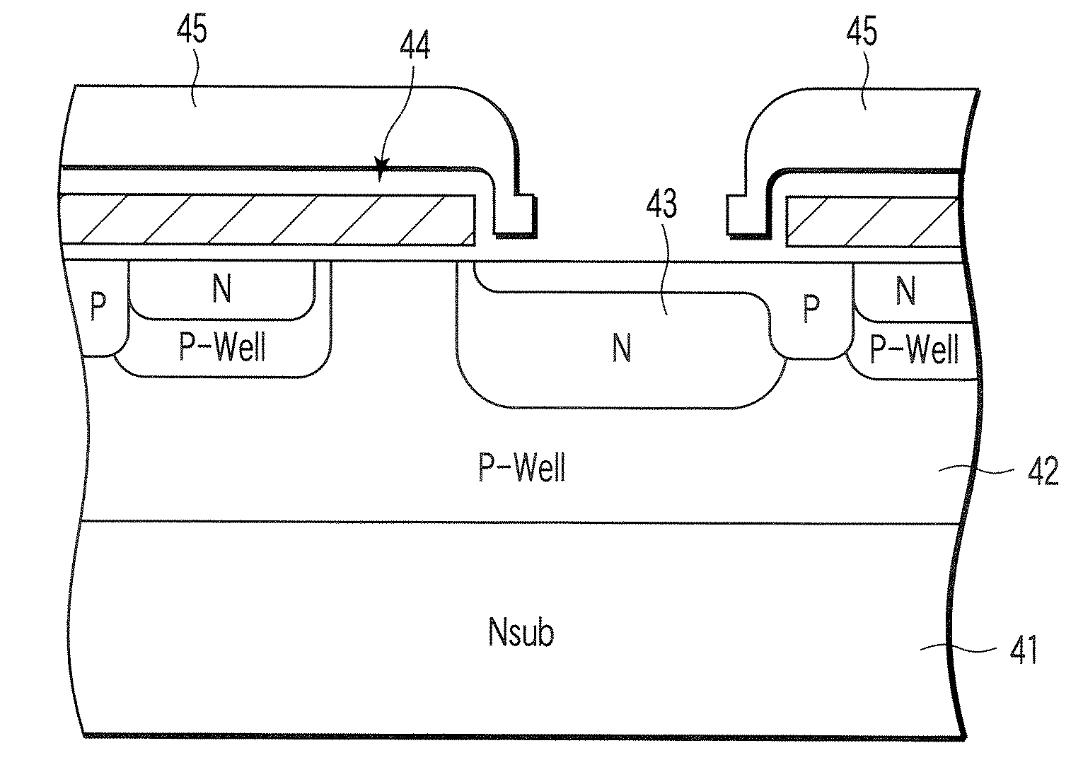
[0101]FIGS. 12A and 12B show a CMOS image sensor according to a third embodiment. FIG. 12A is a cross-sectional view, and FIG. 12B is a circuit diagram. The CMOS image sensor comprises pixel circuits (the circuit is depicted in a region enclosed by a dashed line in FIG. 12B) integrated on the same p-type Si substrate 31. Each pixel circuit includes a photocarrier generation layer 32 comprising an n-type region, an amplifying element 33 that amplifies optical outputs from the photocarrier generation layer 32, a select transistor 34 that selects the pixels, and a reset transistor 35 that resets signal charges. The photocarrier generation layer 32 has basically the same structure as that of the photocarrier generation layer shown in the first embodiment. The amplifying element 33, select transistor 34, and reset transistor 35 are all MOS transistors. The select transistor 34 has a gate electrode connected to a perpendicular select line PSL and a drain connected to a signal line SIG. Th...
PUM
 Abstract
Description
Claims
Application Information
 - R&D
- Intellectual Property
- Life Sciences
- Materials
- Tech Scout
- Unparalleled Data Quality
- Higher Quality Content
- 60% Fewer Hallucinations
Browse by: Latest US Patents, China's latest patents, Technical Efficacy Thesaurus, Application Domain, Technology Topic, Popular Technical Reports.
© 2025 PatSnap. All rights reserved.Legal|Privacy policy|Modern Slavery Act Transparency Statement|Sitemap|About US| Contact US: help@patsnap.com


