Nonvolatile memory device

Active Publication Date: 2007-11-22
RENESAS ELECTRONICS CORP
View PDF10 Cites 43 Cited by
  • Summary
  • Abstract
  • Description
  • Claims
  • Application Information

AI Technical Summary

Benefits of technology

[0012]The present invention has been made for solving the above-described problems. A first object of the invention is to provide a nonvolatile memory device writing data and reading data by supplying an electric current to a memory cell, for which the read disturb

Problems solved by technology

It is now a particularly important challenge to reduce the cell area of the memory cell in order that such an MRAM device as described above may replace a main memory using a DRAM (Dynamic Random Access Memory) device.
Therefore, if the read current has a large value, an accidental data write occurs, resulting in a problem that the stored data is corrupted.
This phenomenon is called “read disturb.” If the read current value is decreased for avoiding the read disturb, the sense voltage level is also decreased to cause the problem that the da

Method used


Image

  • Nonvolatile memory device
  • Nonvolatile memory device
  • Nonvolatile memory device

Examples


first embodiment

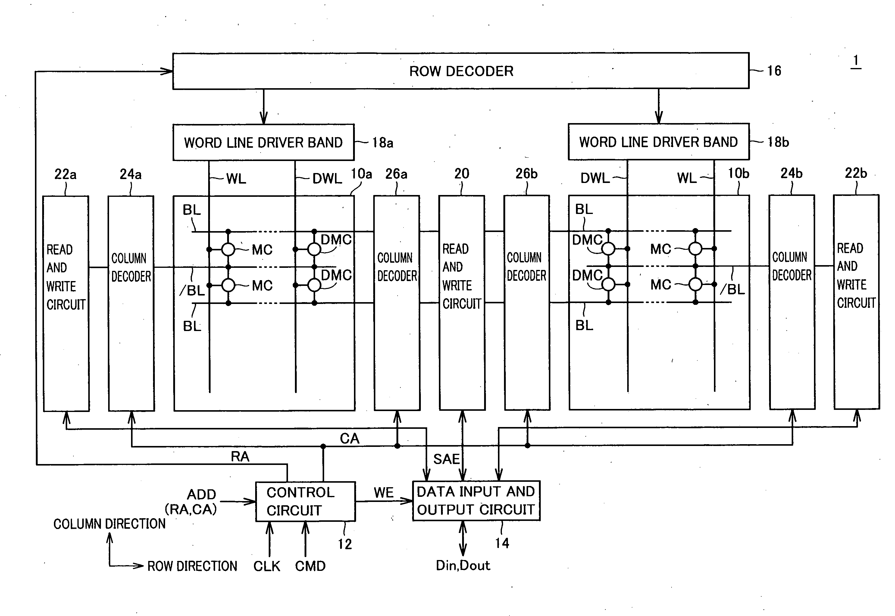
[0041]FIG. 1 shows an entire configuration of an MRAM device 1 that is a typical example of the nonvolatile memory device, according to a first embodiment of the present invention.

[0042]Referring to FIG. 1, in response to externally supplied control signal CMD and address signal ADD, MRAM device 1 makes random access to write input data Din and read output data Dout. The data write operation and the data read operation of MRAM device 1 are performed, for example, at a timing synchronized with externally supplied clock signal CLK. The operation timing may be set internally without receiving clock signal CLK which is externally supplied.

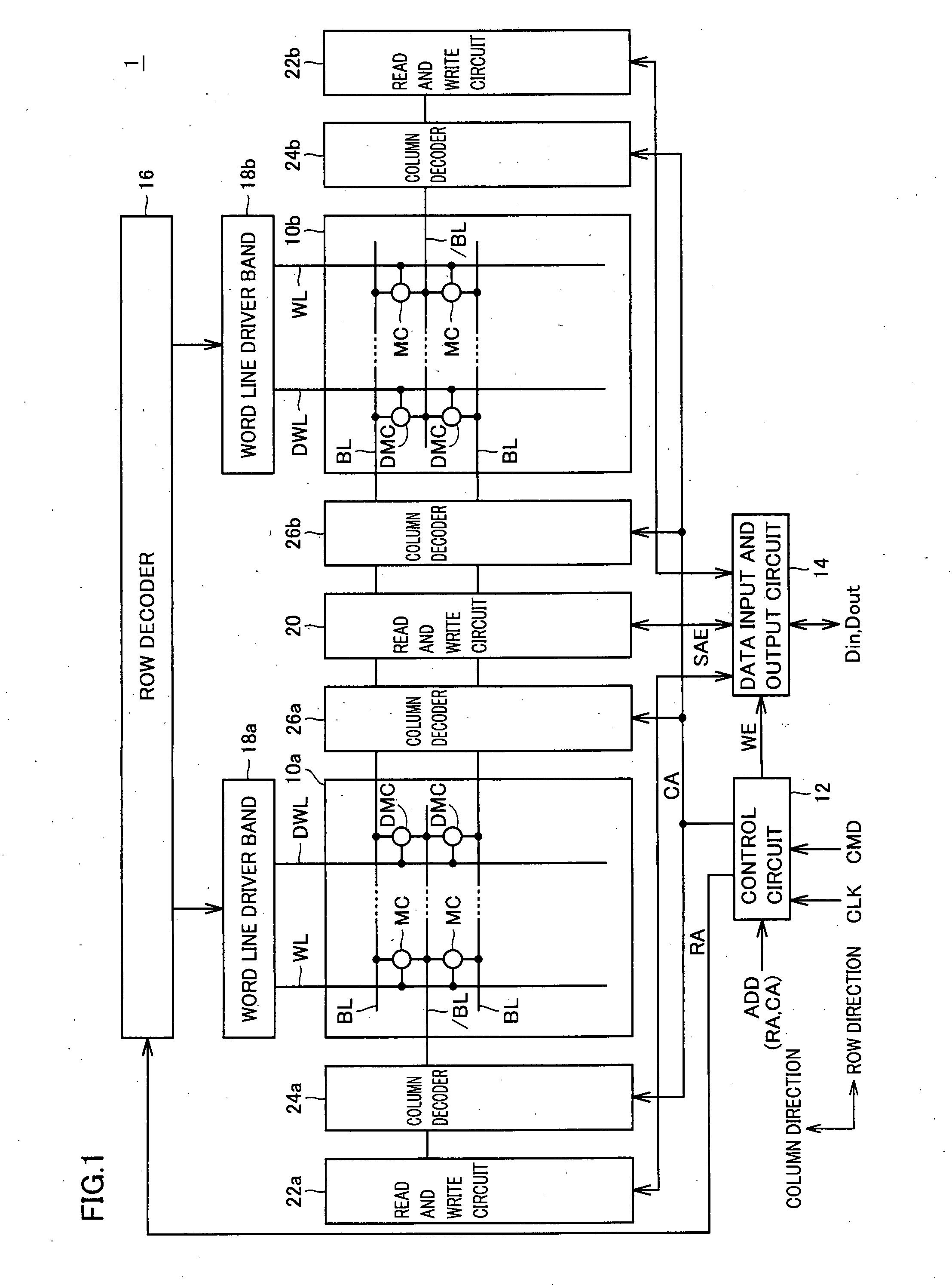
[0043]MRAM device 1 includes a control circuit 12, memory arrays 10a, 10b, a row decoder 16, word line driver bands 18a, 18b, column decoders 24a, 24b, 26a, 26b, a data input and output circuit 14, and read and write circuits 20, 22a, 22b.

[0044]Control circuit 12 controls the whole operation of MRAM device 1 in response to externally supplied control ...

second embodiment

[0156]In connection with the first embodiment, the description is given of the MRAM memory device using the spin injection mechanism where the read current supply duration and the write current supply duration as well as respective values of the read and write currents are optimized in consideration of the thermal assist effect. In connection with a second embodiment, a description is given of an MRAM memory device using the spin injection mechanism where the read current supply direction is optimized in consideration of the thermal assist effect.

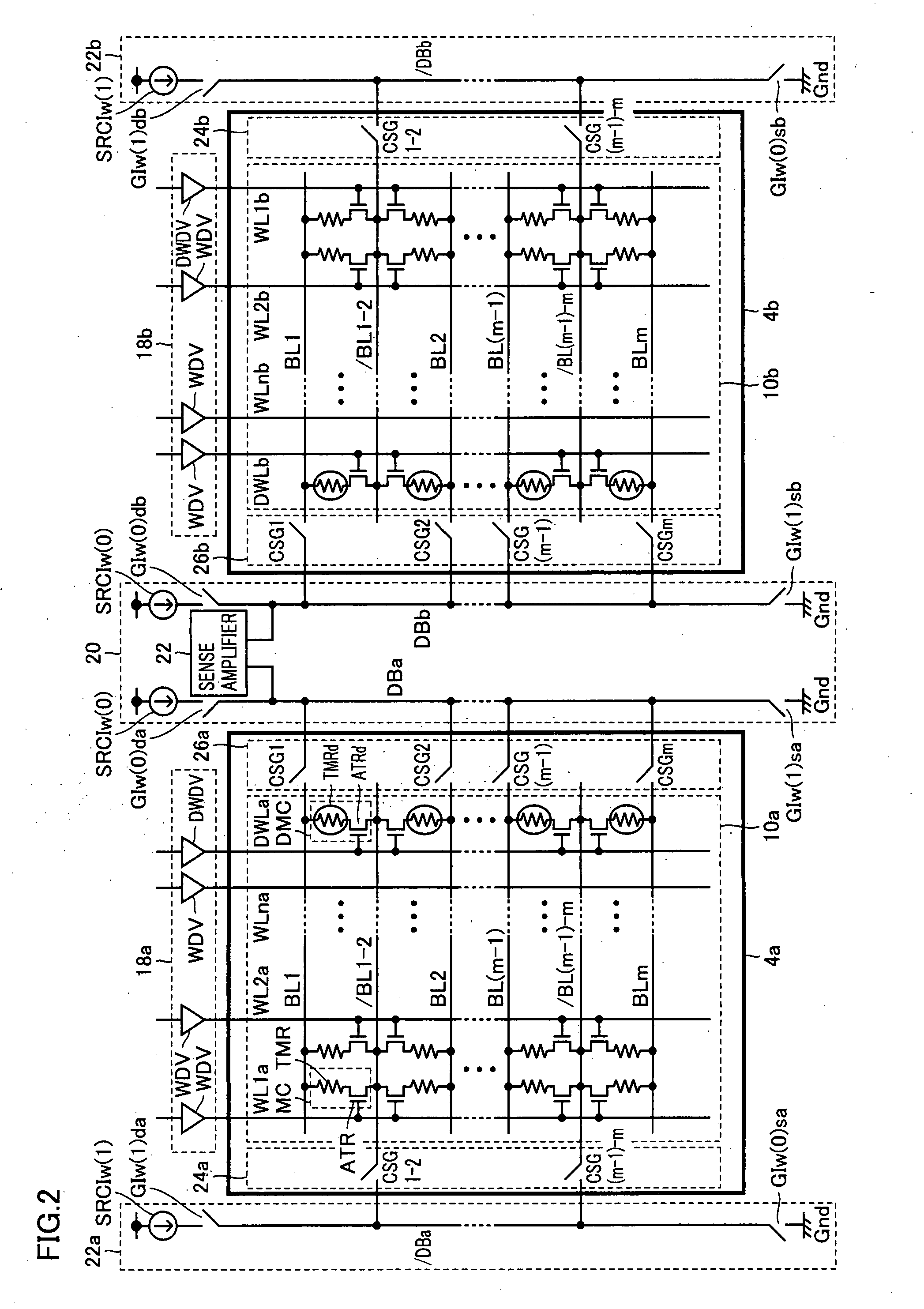
[0157]The entire configuration of the MR device that is a typical example of the semiconductor memory device and the schematic configuration of a memory array and its peripheral circuitry of the second embodiment of the present invention are similar to those in FIGS. 1 and 2 described above. Therefore, the detailed description thereof is not repeated. Further, memory cell MC which is a component of the MRAM device of the second embodiment o...

third embodiment

[0175]In connection with the second embodiment of the present invention, the tunneling magneto-resistance element is described for which there is a difference between the absolute value of the write current required for changing the electric resistance value from the high resistance state to the low resistance state and the absolute value of the write current required for changing the electric resistance value from the low resistance state to the high resistance state. In contrast, in connection with a third embodiment of the present invention, a tunneling magneto-resistance element is described for which respective absolute values of write currents required for causing the electric resistance value to the high and low resistance states are substantially equal to each other.

[0176]The entire configuration of the MRAM device that is a typical example of the nonvolatile memory device of the third embodiment and the schematic configuration of a memory array and its peripheral circuitry ...


PUM


Abstract

Between the value of an electric current and the supply duration for which the electric current is supplied that cause magnetization reversal, there is the relation of monotonous decrease. This means that, as the supply duration is shortened, the threshold current value for causing the magnetization reversal is larger. Therefore, in terms of suppressing occurrence of read disturb, the read current supply duration may be shortened to increase the threshold value of the current causing the magnetization reversal and thereby ensure a sufficient read disturb margin. Therefore, the read current supply duration may be shortened relative to the write current supply duration ensure the read disturb margin and suppress occurrence of read disturb.

Description

BACKGROUND OF THE INVENTION[0001]1. Field of the Invention[0002]The present invention relates to a nonvolatile memory device. In particular, the invention relates to a random-access memory including memory cells having magnetic tunnel junctions (MTJ).[0003]2. Description of the Background Art[0004]In recent years, an MRAM (Magnetic Random-Access Memory) device has been of great interest as a new-generation nonvolatile memory device. The MRAM device is a nonvolatile memory device in which a plurality of thin-film magnetic elements formed in a semiconductor integrated circuit are used to store data in nonvolatile manner, and the thin-film magnetic elements are each randomly accessible. In particular, recently it has been known that an MRAM device is remarkably improved in performance by employment of the thin-film magnetic element using a magnetic tunnel junction (MTJ) as a memory cell.[0005]Generally, when data is to be read from a memory cell configured using such a thin-film magnet...

Claims


Application Information

Patent Timeline
IPC IPC(8): G11C11/00
CPCG11C11/16G11C11/1653G11C11/1673G11C11/1675G11C11/1677G11C11/1693
Inventor HIDAKA, HIDETO
Owner RENESAS ELECTRONICS CORP
Why Eureka
Try Eureka