

Scanning probe microscope probe and manufacturing method therefor, scanning probe microscope and using method therefor, needle-like body and manufacturing method therefor, electronic device and manufacturing method therefor, charge density wave quantum phase microscope, and charge density wave quantum interferometer
- Summary
- Abstract
- Description
- Claims
- Application Information
AI Technical Summary
Benefits of technology
Problems solved by technology
Method used
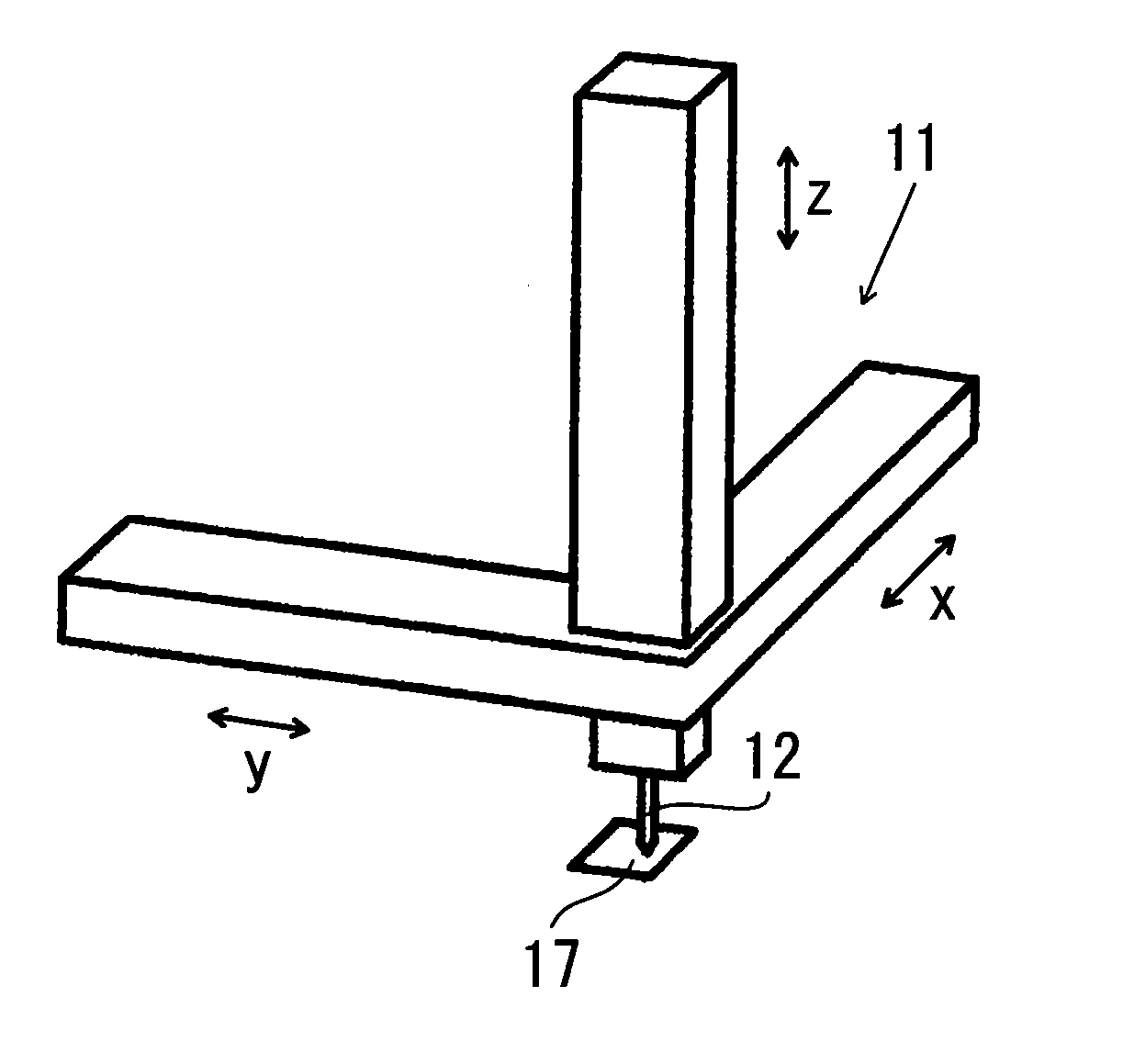
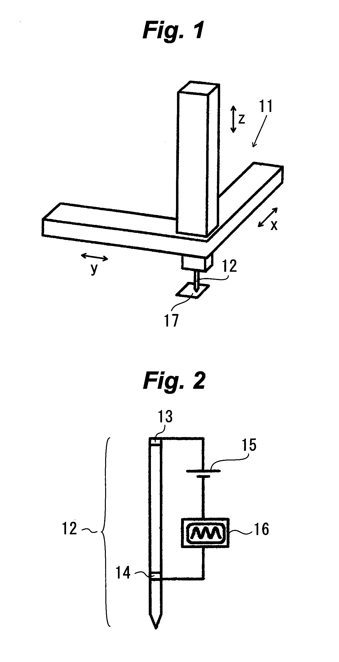
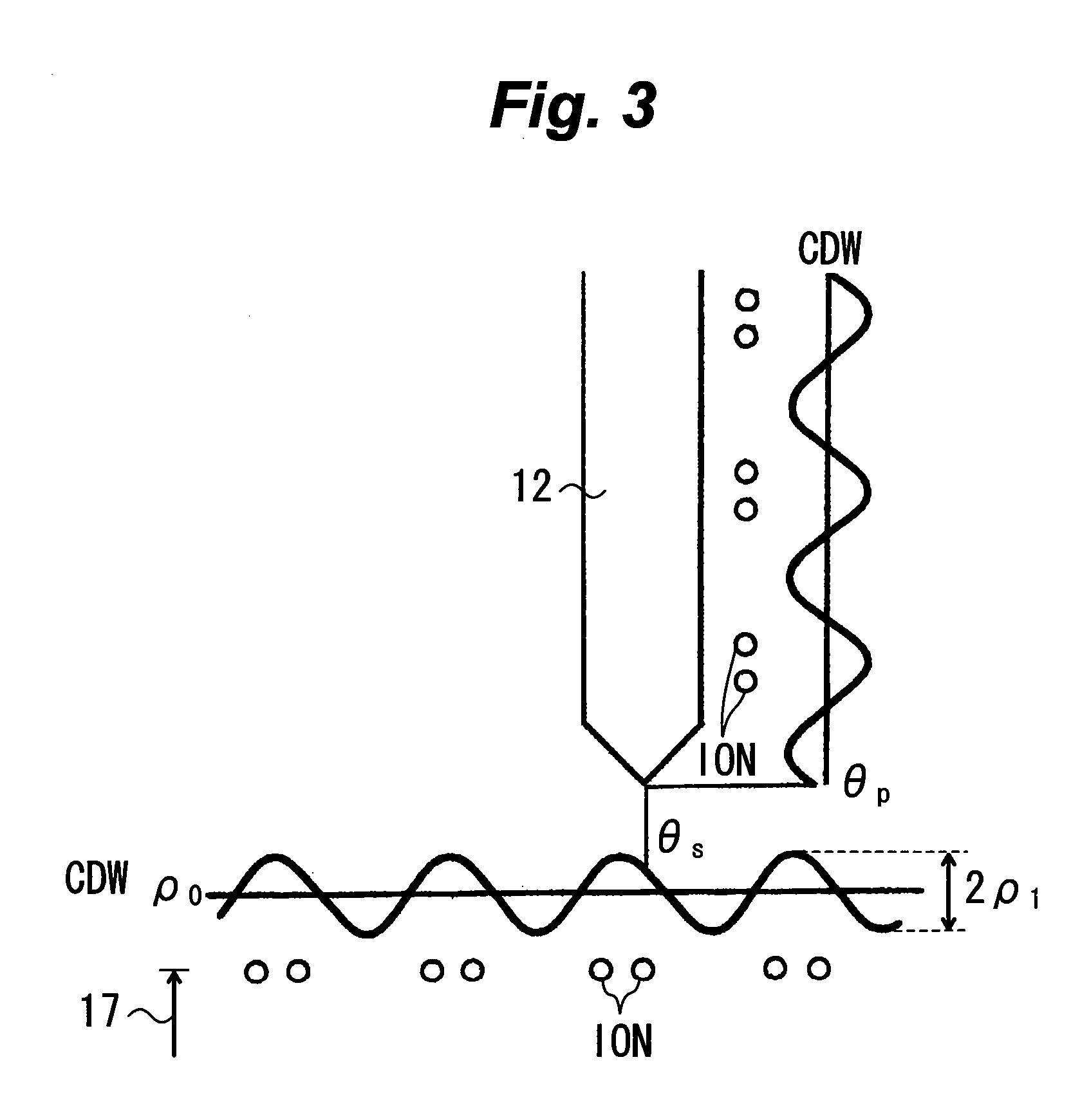
Image

Examples
example 1
[0102] After the Ta and Se films were formed one after another by the vacuum evaporation on the surface of the cone 21 made of Si, the electron beam 23 was irradiated to a point on the cone 21 at a distance of L=2 μm along the surface from the tip of the cone 21 having the raw-material film 22 formed from the Ta and Se films. The Ta film was 100 nm in thickness and Se film was 200 nm in thickness. The spot size of the electron beam 23 was 1 μm, acceleration voltage was 25 kV, irradiation current amount was 1×10⁻⁷ μA and irradiation time was 30 min. Also, the electron beam 23 was irradiated in a vacuum of 3 to 4×10⁻⁶ Torr. As a result, a needle-like crystal of TaSe2 was grown to a diameter of about 0.4 μm and length of about 1.5 μm at a point at a distance of about 0.5 μm from the cone tip. FIG. 5 is a scanning electron microscope (SEM) micrograph of the needle-like crystal. In this case, it is considered that the point on the cone 21, irradiated with the electron beam 23, had a temp...
example 2
[0150] The electron beam 23 was irradiated to the predetermined point on the surface of the CDW crystal substrate 91 formed from the TaSe2 crystal. The CDW crystal substrate 91 has a square shape of which each side is about 40 μm long. The electron beam 23 was irradiated to a spot of 1 μm in size with an irradiation current of 8×10⁻⁸ A at an acceleration voltage of 25 kV for 30 min. Also, the electron beam 23 was irradiated in a vacuum of 3 to 4×10⁶ Torr. As the result, the CDW needle-like crystal 24 made of the single crystal TaSe2 needle-like crystal (nano-fiber) of about 50 nm in diameter was grown to a length of about 150 nm contiguously with the CDW crystal substrate 91 on the CDW crystal substrate 91 made of the TaSe2 crystal.
[0151] According the eleventh embodiment, the CDW needle-like crystal 24 suitable for use in a CDW quantum phase microscope can be provided.
[0152] The Andreev-reflection scanning probe microscope according to the twelfth embodiment of the present invent...
PUM
| Property | Measurement | Unit |
|---|---|---|
| Pressure | aaaaa | aaaaa |
| Density | aaaaa | aaaaa |
| Height | aaaaa | aaaaa |
Abstract
Description
Claims
Application Information