

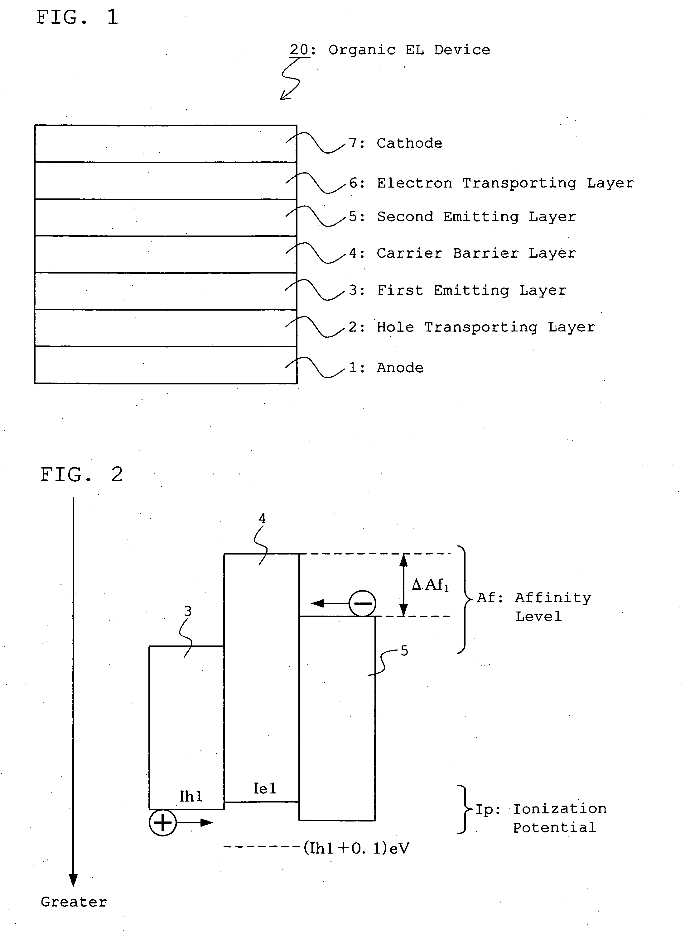
Organic electroluminescence device
an electroluminescent device and organic technology, applied in the direction of discharge tube luminescnet screen, triarylamine dye, anthracene dye, etc., can solve the problems of insufficient luminous efficiency high driving voltage of organic el device, etc., to achieve small chromaticity change and high luminous efficiency
- Summary
- Abstract
- Description
- Claims
- Application Information
AI Technical Summary
Benefits of technology
Problems solved by technology
Method used
Image

Examples
example 1
(Fabrication of Organic EL Device)
[0246]A grass substrate of 25 mm by 75 mm by 1.1 mm thick with an ITO transparent electrode (anode) (GEOMATEC CO., LTD.) (thickness of ITO was 130 nm) was subjected to ultrasonic cleaning with isopropyl alcohol for 5 minutes, and cleaned with ultraviolet rays and ozone for 30 minutes. The resultant substrate with transparent electrode lines was mounted on a substrate holder in a vacuum deposition device. First, an HI film was formed in a thickness of 60 nm so as to cover the surface of the transparence electrode on which the transparence electrode lines were formed. This HI film functioned as a hole-injecting layer. After forming the HI film, an HT film was formed in a thickness of 15 nm on the HI film. This HT film functioned as a hole-transporting layer.
[0247]Following the formation of the HT film, RH (Eg: 2.4 eV) and RD were deposited to a thickness of 5 nm to form a first emitting layer (Ip / Af [eV]=5.6 / 3.2) such that the concentration of RD was ...
example 2
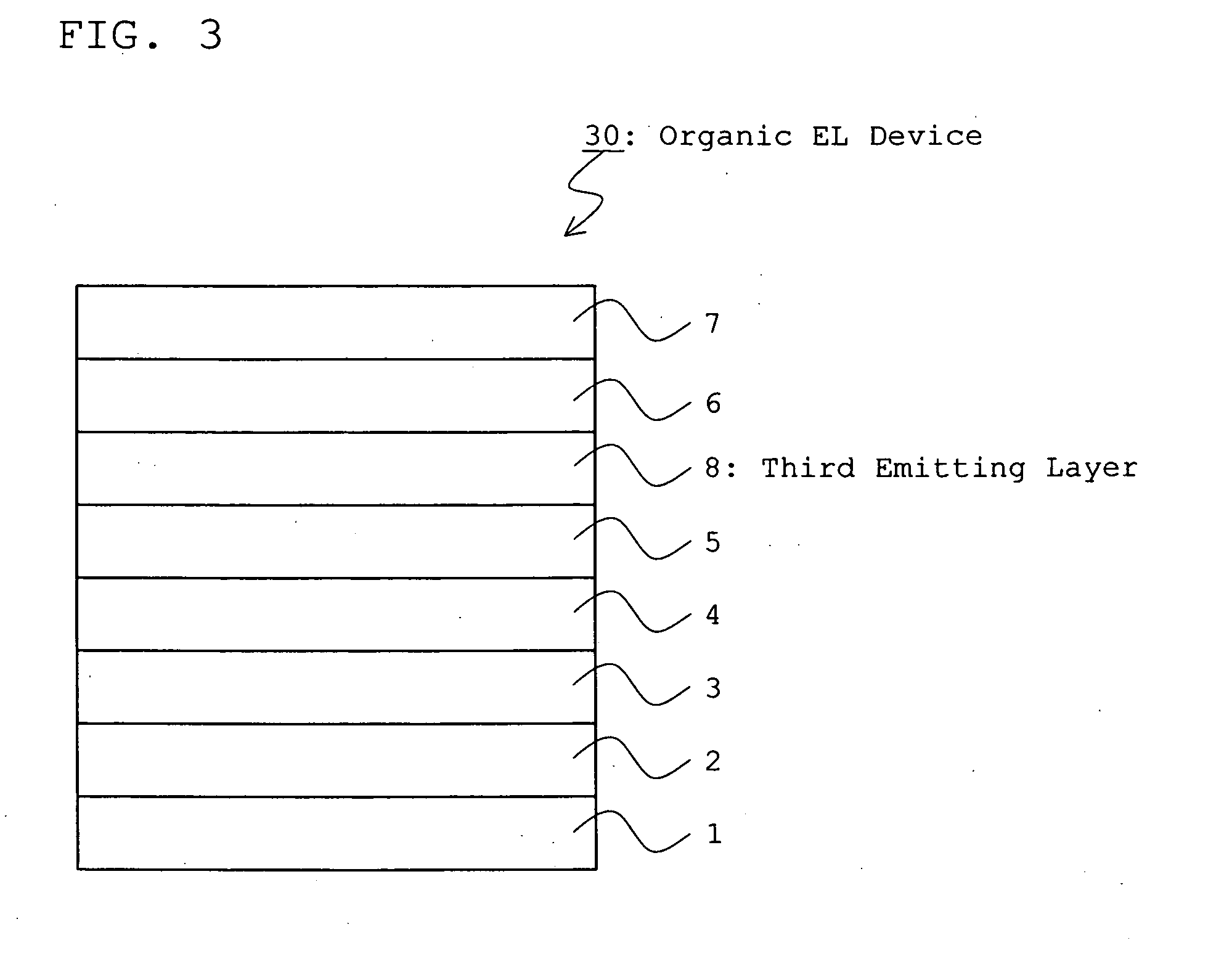
[0253]An organic EL device was fabricated in the same way as in Example 1 except that after forming the second emitting layer in a thickness of 10 nm, as a third emitting layer, BH and GD were deposited to a thickness of 30 nm to form a green emitting layer (Ip / Af [eV]=5.8 / 2.8) such that the concentration of GD was 10 wt % and then the Alq3 layer (electron transporting layer) was formed. The organic EL device obtained was measured in the same way as in Example 1. The results were shown in Table 1.
example 3
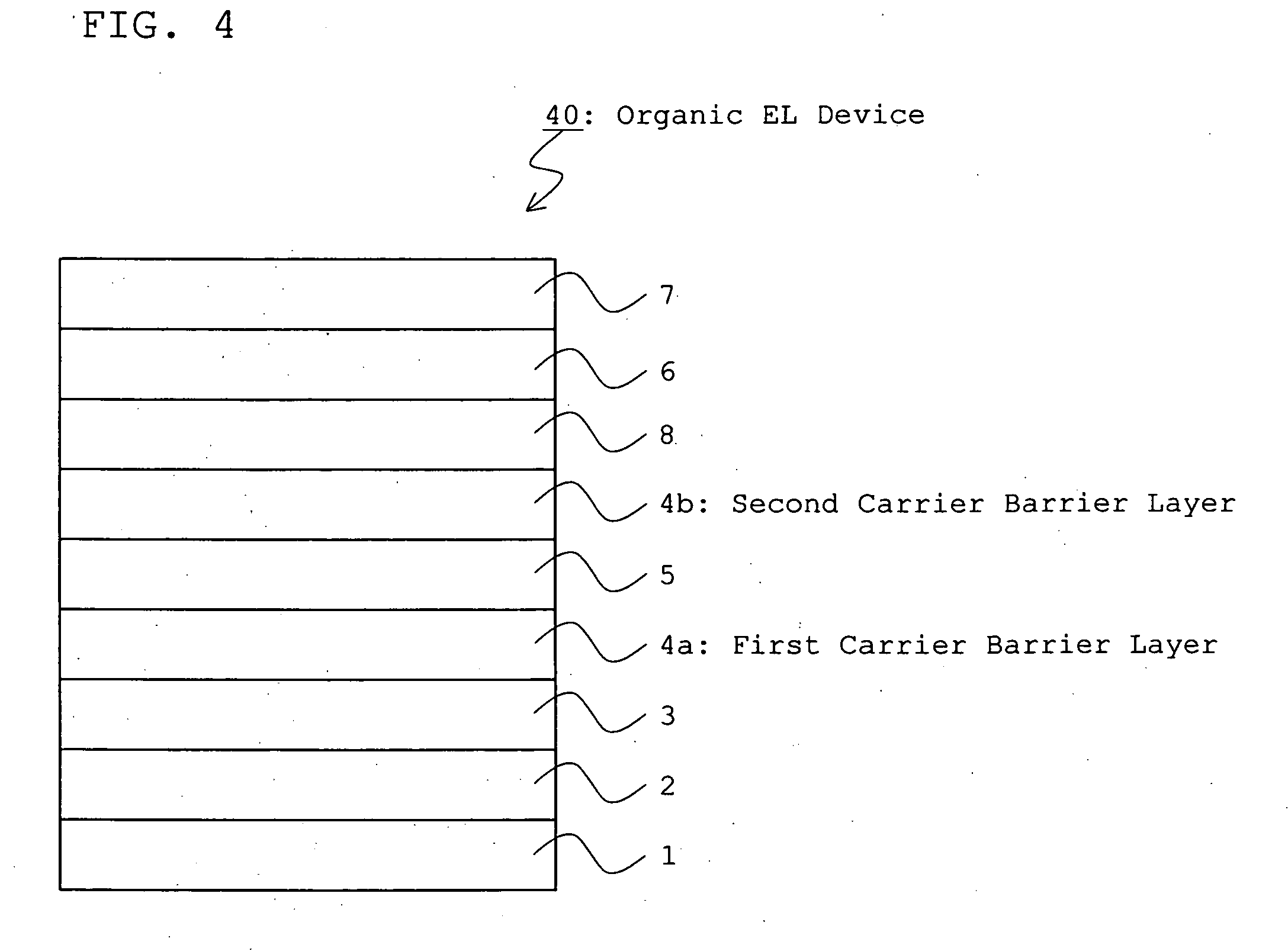
[0255]An organic EL device was fabricated in the same way as in Example 1 except that as the carrier barrier layer, HT and GD were deposited instead of HT to form a layer (Ip / Af [eV]=5.36 / 2.3) such that the concentration of GD was 10 wt %, and the thickness of the second emitting layer was changed to 40 nm.
[0256]The organic EL device obtained was measured in the same way as in Example 1. The results were shown in Table 1.
PUM
| Property | Measurement | Unit |
|---|---|---|
| Energy | aaaaa | aaaaa |
| External quantum efficiency | aaaaa | aaaaa |
| External quantum efficiency | aaaaa | aaaaa |
Abstract
Description
Claims
Application Information