Nonvolatile semiconductor memory device

a semiconductor memory and non-volatile technology, applied in semiconductor devices, electrical devices, instruments, etc., can solve the problem of increasing the writing voltage, and achieve the effect of reducing the leakage of charge retained in the charge storage layer into the semiconductor layer, improving the charge retention property of the charge storage layer, and easy retention of charg

Inactive Publication Date: 2007-12-06
SEMICON ENERGY LAB CO LTD
View PDF16 Cites 80 Cited by
  • Summary
  • Abstract
  • Description
  • Claims
  • Application Information

AI Technical Summary

Benefits of technology

[0018]When different nitride compound layers are stacked over a semiconductor region (a semiconductor layer or a semiconductor substrate) with a first insulating layer serving as a tunnel insulating layer interposed therebetween and at least one or more of the nitride compound layers serve as charge storage layers, a plurality of sites (traps) for retaining charge is included in at least one of the different nitride compound layers or at an interface between the different nitride compound layers; accordingly, charge is easily retained. In addition, when a layer formed of...

Problems solved by technology

When such a difference in the energy level is generated, injection of electrons into the floati...

Method used


Image

  • Nonvolatile semiconductor memory device
  • Nonvolatile semiconductor memory device
  • Nonvolatile semiconductor memory device

Examples


embodiment mode 1

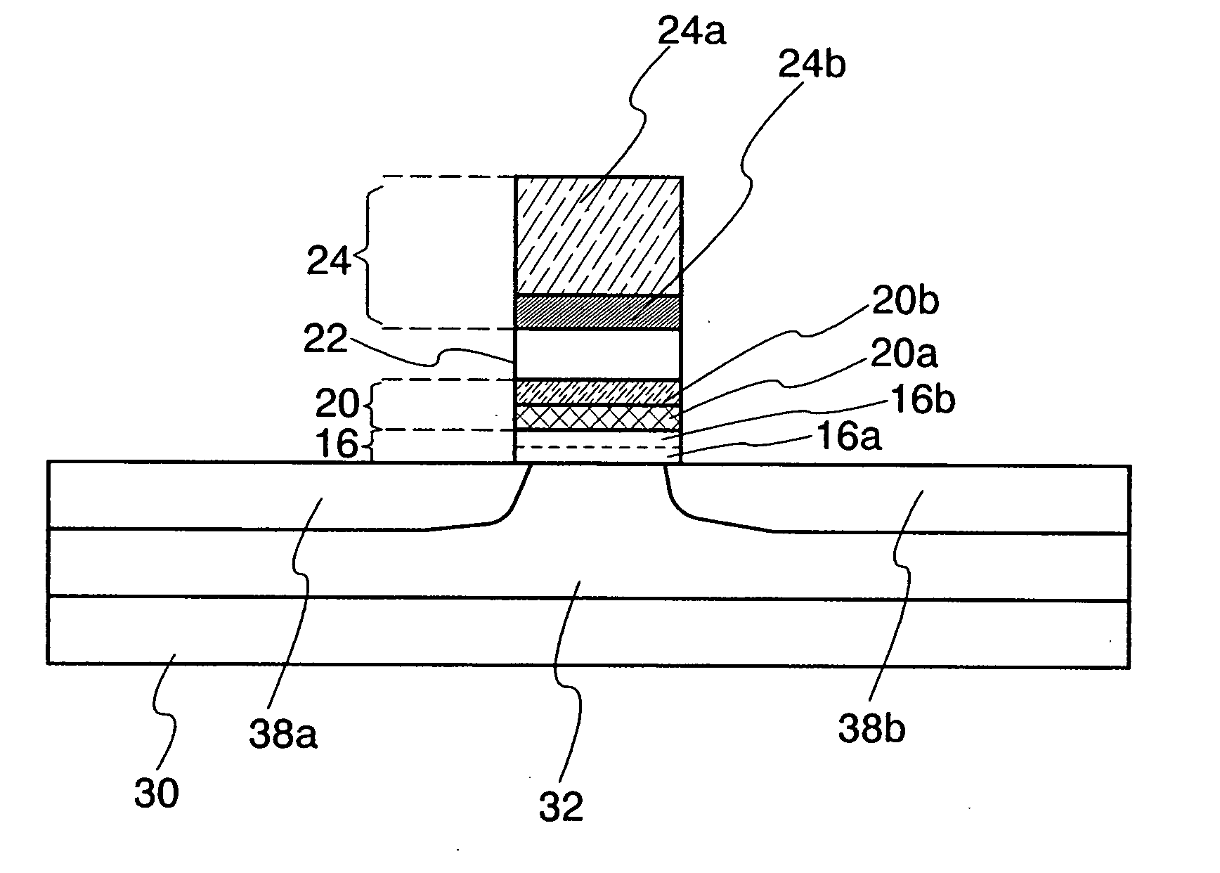
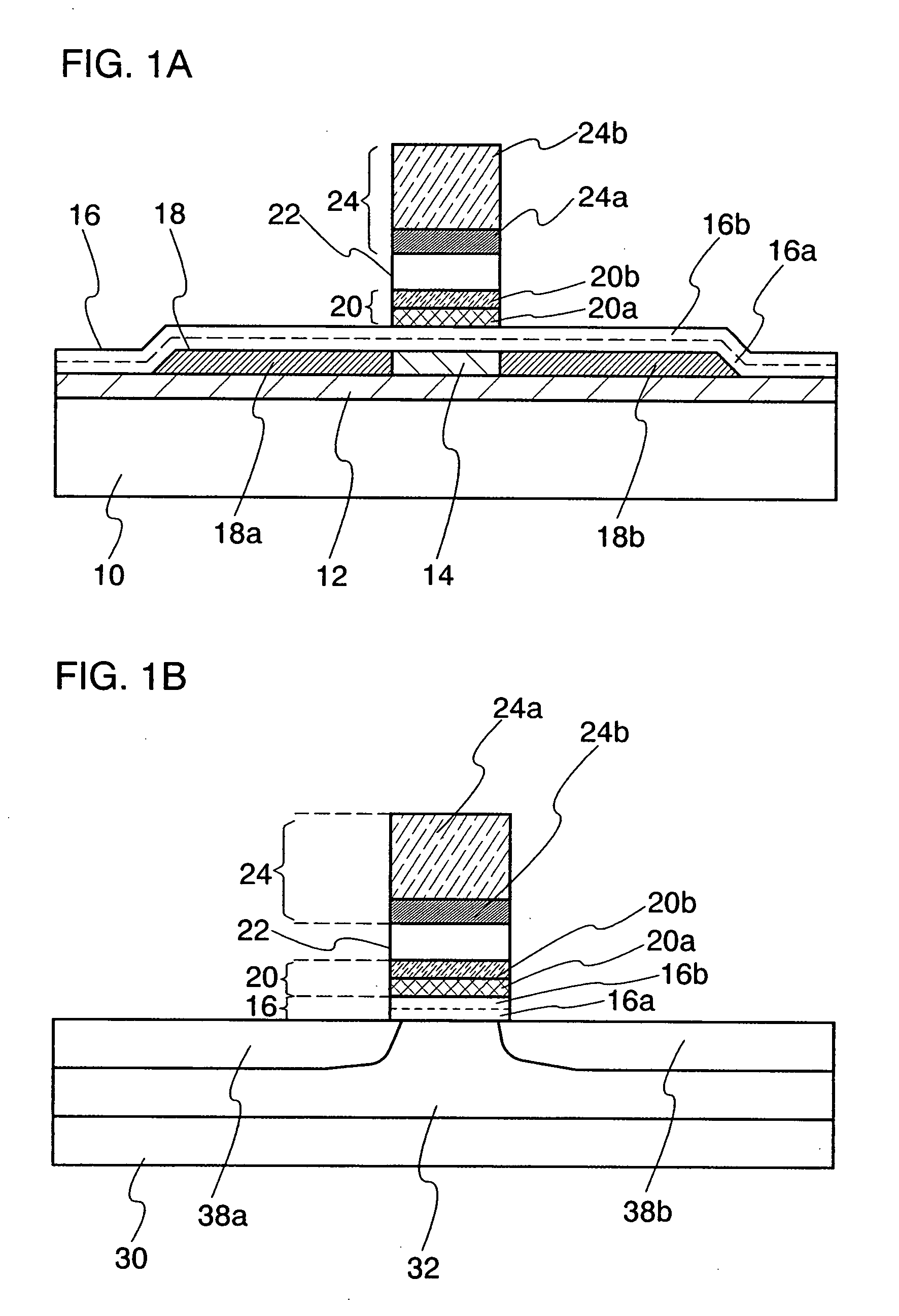
[0078]FIGS. 1A and 1B are each a cross-sectional view for explaining a main structure of a nonvolatile semiconductor memory device of the present invention. In particular, FIG. 1A shows a main portion of a nonvolatile memory element. This nonvolatile memory element is formed using a substrate 10 having an insulating surface. As the substrate 10 having the insulating surface, a glass substrate, a quartz substrate, a sapphire substrate, a ceramic substrate, a metal substrate over which an insulating layer is formed, or the like can be used.

[0079]A semiconductor layer 18 is formed over the substrate 10 having the insulating surface. An insulating layer 12 serving as a base film may be provided between the substrate 10 and the semiconductor layer 18. This insulating layer 12 prevents an impurity such as alkali metal from diffusing into the semiconductor layer 18 from the substrate 10 and contaminating the semiconductor layer 18, and may be appropriately provided as a blocking layer.

[008...

embodiment mode 2

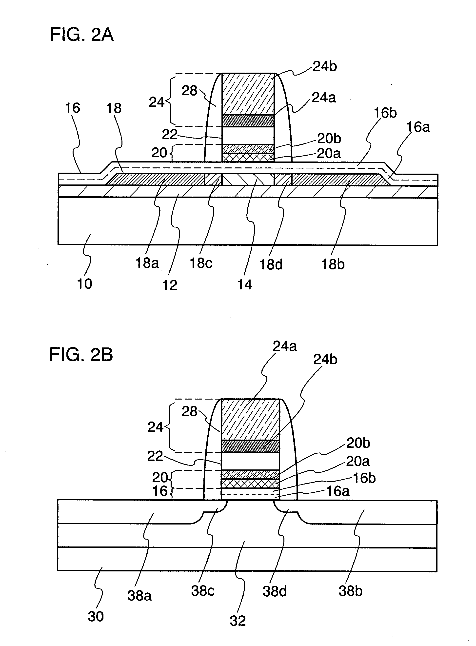
[0147]In this embodiment mode, a structure of the nonvolatile memory element of the above-described embodiment mode will be hereinafter explained, in which effects on the characteristics of the nonvolatile memory element due to a coverage defect of a first insulating layer 16 at edges of a semiconductor layer 18, storage of charge in a manufacturing process, or the like, especially, effects on the characteristics of the nonvolatile memory element due to a coverage defect when the first insulating layer 16 is thin, storage of charge in a manufacturing process, or the like can be reduced.

[0148]FIG. 51A shows a top view of a nonvolatile memory element, and FIG. 51B and FIG. 51C are schematic cross-sectional views taken along a line A1-B1 and a line A2-B2 of FIG. 51A, respectively.

[0149]In the structure shown in FIGS. 51A to 51C, the island-shaped semiconductor layer 18 includes the channel formation region 14 which is provided in a region overlapping with the control gate electrode 24,...

embodiment 1

[0162]In this embodiment, an example of a nonvolatile semiconductor memory device will be explained with reference to drawings. Here, the case where, in the nonvolatile semiconductor memory device, a nonvolatile memory element for forming a memory portion and an element such as a transistor for forming a logic portion, which is formed over the same substrate as the memory portion and performs control of the memory portion, or the like are formed at the same time will be explained.

[0163]First, a schematic view of the memory portion in the nonvolatile semiconductor memory device is shown in FIG. 8.

[0164]In the memory portion shown in this embodiment, a plurality of memory cells each of which have a controlling transistor S and a nonvolatile memory element M is provided. In FIG. 8, one memory cell is formed of a controlling transistor S01 and a nonvolatile memory element M01. In addition, similarly, a memory cell is formed of a controlling transistor SO2 and a nonvolatile memory elemen...


PUM


Abstract

An object is to provide a nonvolatile semiconductor memory device which is excellent in a writing property and a charge retention property. In addition, another object is to provide a nonvolatile semiconductor memory device capable of reducing writing voltage. A nonvolatile semiconductor memory device includes a semiconductor layer or a semiconductor substrate including a channel formation region between a pair of impurity regions that are formed apart from each other, and a first insulating layer, a plurality of layers formed of different nitride compounds, a second insulating layer, and a control gate that are formed in a position which is over the semiconductor layer or the semiconductor substrate and overlaps with the channel formation region.

Description

BACKGROUND OF THE INVENTION[0001]1. Field of the Invention[0002]The present invention relates to a nonvolatile semiconductor memory device capable of electrical writing, reading, and erasing, and a manufacturing method thereof. In particular, the present invention relates to a structure of a charge storage layer in the nonvolatile semiconductor memory device.[0003]2. Description of the Related Art[0004]A market of nonvolatile memory capable of electrically rewriting data and storing data even when power is turned off has been expanded. The nonvolatile memory has a similar structure to that of MOSFET (Metal Oxide Semiconductor Field Effect Transistor) and has a feature in that a region capable of storing charge for a long period of time is provided over a channel formation region. This charge storage region is formed over an insulating layer and is insulated and isolated from a peripheral region; accordingly, the charge storage region is referred to as a floating gate. A control gate...

Claims


Application Information

Patent Timeline
IPC IPC(8): H01L29/792
CPCG11C16/0416G11C16/0433G11C16/0483H01L21/28282H01L21/84H01L27/115H01L29/792H01L27/11546H01L27/12H01L27/1203H01L29/4234H01L29/513H01L27/11526H01L29/40117H10B69/00H10B41/40H10B41/49H01L21/28202
Inventor TAKANO, TAMAETOKUDA, ATSUSHITAJIMA, RYOTAYAMAZAKI, SHUNPEI
Owner SEMICON ENERGY LAB CO LTD
Why Eureka
Try Eureka