

Flap Type Nano/Micro Mechanical Device and Fabrication Method Thereof
a nano-micro and mechanical device technology, applied in piezoelectric/electrostrictive/magnetostrictive devices, oscillation generators, impedence networks, etc., can solve the problems of low current detection, large magnetic field, and inability to measure the motion of mechanical devices, etc., to achieve precise control of the thickness of the dielectric layer, control the effect of nanometer precision and simple and precise manner
Inactive Publication Date: 2007-12-06
SEIKO EPSON CORP
View PDF5 Cites 8 Cited by
- Summary
- Abstract
- Description
- Claims
- Application Information
AI Technical Summary
Benefits of technology
[0005] It is an object of the present invention to overcome the above-described drawbacks of prior art by providing a capacitative-based device having micro and nanometer scale dimensions, that is easy to manufacture and that can have resonant frequencies in the GHz range, and in which the current generated by the device is enhanced.
Problems solved by technology
A main problem of scaling down the dimensions of such devices that is needed to reach the desired frequencies, has been the possibility of measuring the motion of the mechanical device, due to oscillation amplitudes in the nm to sub-nm range.
This does however involve the disadvantages of requiring large magnetic fields and low current detection which both require helium temperatures (4.8K).
Whilst this allows to avoid the need of operating at low temperatures, until now only very low current signals have been measured and fabrication of these devices that are based on radial vibrating disk resonators, is very complex, so that it is difficult to integrate them with integrated circuits.
Method used
View moreImage
Smart ImageViewing Examples

Examples
first embodiment
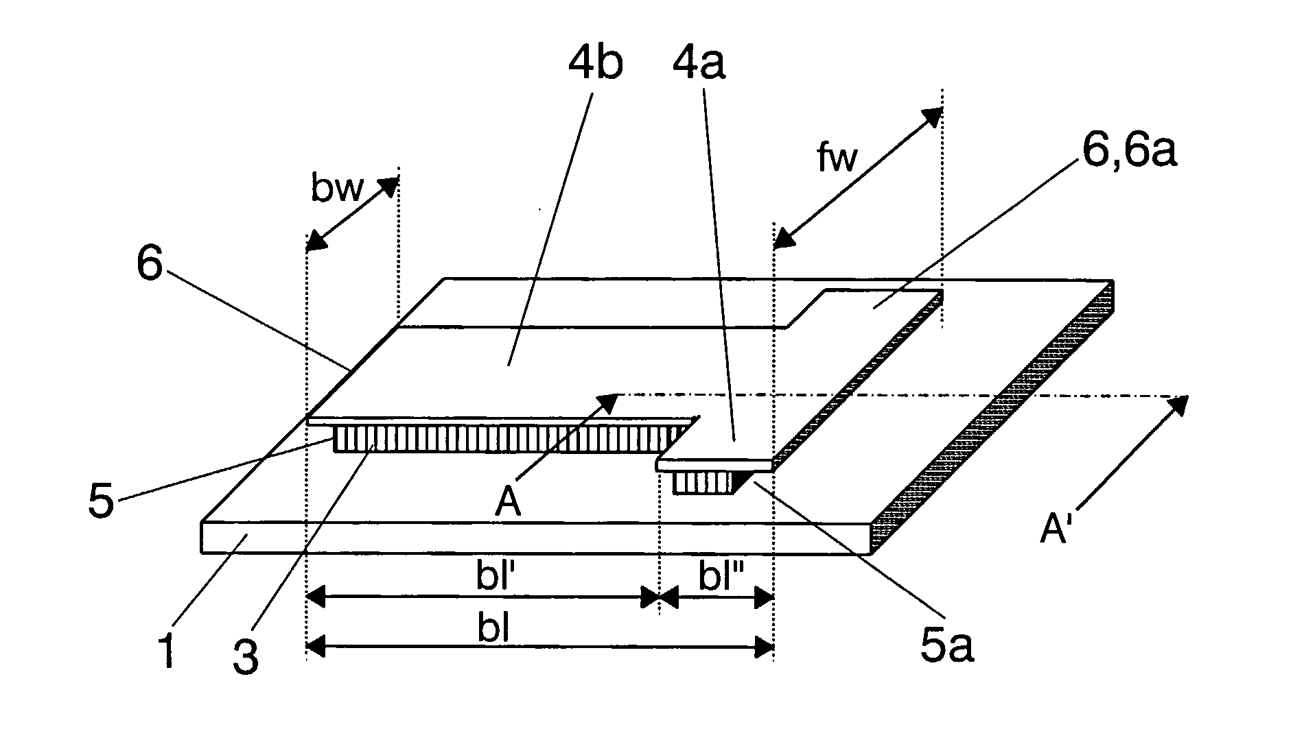
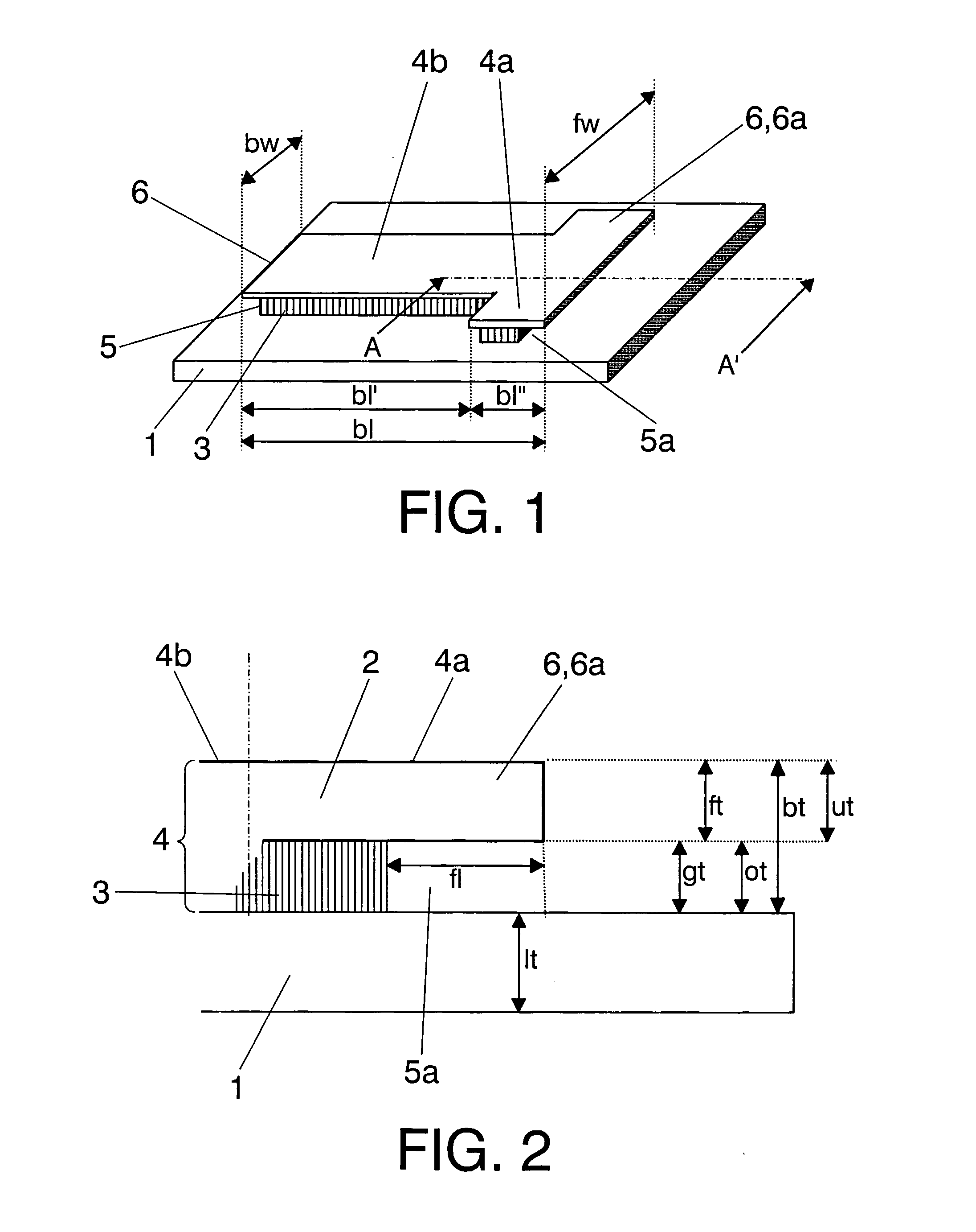
[0029]FIG. 1 is a lateral perspective view that schematically shows the device of the present invention in accordance with a first embodiment;
[0030]FIG. 2 is a cross sectional view along line A-A′ of the device shown in FIG. 1;
second embodiment
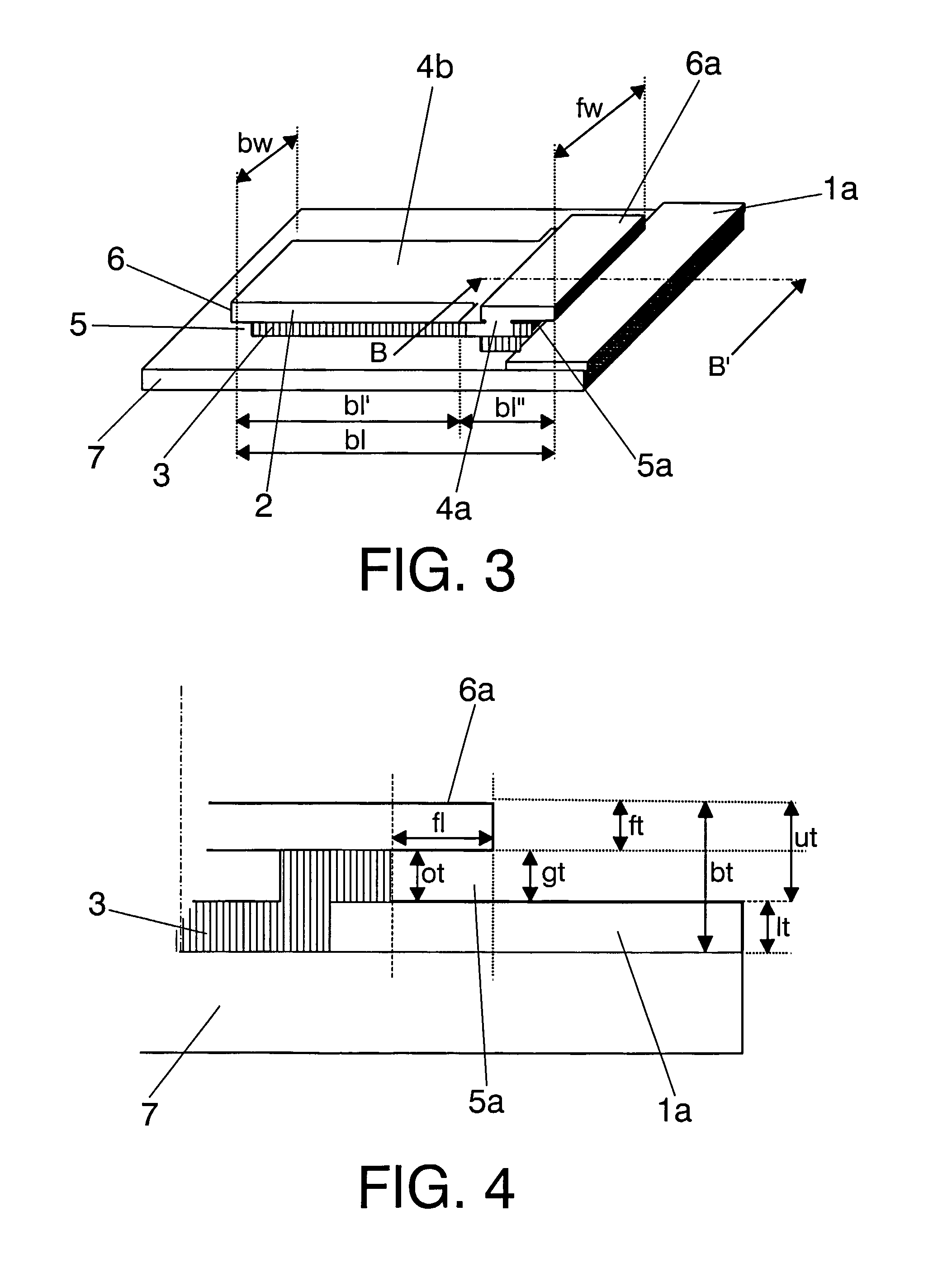
[0031]FIG. 3 is a lateral perspective view that schematically shows the device of the present invention in accordance with a second embodiment;
[0032]FIG. 4 is a cross sectional view along line B-B′ of the device shown in FIG. 3;
third embodiment
[0033]FIG. 5 is a lateral perspective view that schematically shows the device of the present invention in accordance with a third embodiment;
[0034]FIG. 6 is a cross sectional view along line C-C′ of the device shown in FIG. 5;
Login to View More PUM
| Property | Measurement | Unit |
|---|---|---|
| width | aaaaa | aaaaa |
| length | aaaaa | aaaaa |
| thickness | aaaaa | aaaaa |
Abstract
A μ-flap type nano / micro mechanical device with a lower electrode 1,1a, 1b, an upper electrode layer 2, an dielectric layer 3 arranged between the lower electrode 1,1a,1b and the upper layer 2, such that the dielectric layer 3 and said upper electrode layer—2 form a layered body 4, the layered body 4 comprising a horizontal recess 5 in a side portion of the dielectric layer 3, and an overhanging portion 6 of reduced thickness over the recess 5 that forms a gap 5a; such that the overhanging portion 6 forms a μ-flap 6a which extends over the gap 5a. The device is a capacitative-based device in which the mechanical motion can be measured at room temperature and without monolithic integration thereof with an integrated circuit but that can be easily integrated with complementary metal oxide semiconductor (CMOS) circuitry.
Description
TECHNICAL FIELD OF THE INVENTION [0001] The present invention belongs to the technical field of integrated circuits and, more particularly, to high frequency mechanical resonators having dimensions in the nano / micrometer scale. PRIOR ART TO THE INVENTION [0002] In electronics, radiofrequency mechanical resonators have since some time ago been considered to be a suitable way to minimize size, power and cost, as well as to maximize functionality. Devices in the micro- and nano-meter scale having fundamental Eigen-frequencies in the MHz and GHz range have been developed for such purpose in recent years. By minimizing the size of such devices, the effective mass compared to the spring constant is substantially reduced, which increases the resonant frequency. A main problem of scaling down the dimensions of such devices that is needed to reach the desired frequencies, has been the possibility of measuring the motion of the mechanical device, due to oscillation amplitudes in the nm to su...
Claims
Login to View More Application Information
Patent Timeline
 Patent Type & AuthorityApplications(United States)
IPC IPC(8): H03B5/30H01S4/00B81B3/00H03H3/007H03H9/24
CPCH03H3/0072Y10T29/49002H03H9/2457
InventorDAVIS, ZACHARY JAMES
OwnerSEIKO EPSON CORP