Photovoltaic interconnect wire

a photovoltaic interconnect wire and interconnect wire technology, applied in the direction of manufacturing tools, welding/cutting media/materials, welding apparatus, etc., can solve the problems of reducing the soldering firmness the surface of the interconnect wire not having pits to protrude, and the inability to efficiently reflect sunlight, so as to improve the total reflection proportion of sunlight incident, the effect of reducing the loss of the effective cross-section area of the conductive bas

Active Publication Date: 2016-11-17
FUNDANT JIANGSU ADVANCED MATERIALS CO LTD
View PDF6 Cites 1 Cited by
  • Summary
  • Abstract
  • Description
  • Claims
  • Application Information

AI Technical Summary

Benefits of technology

[0026]The photovoltaic interconnect wire of the invention can realize a comprehensive balance in at least the following four aspects, by considering real needs of customers, to benefit of the customers to the most: 1) the overall effective output power of the photovoltaic module is increased by improving the total reflection proportion of sunlight incident onto the interconnect wire; 2) the interconnect wire and the solar cell are firmly soldered together by adjusting the proportion of the total area of the flat base strip regions to the total area of the base strip; 3) loss in effective cross-section area of the conductive base strip is reduced by adjusting the angle of the grooves, so as to minimize the loss in current collection efficiency of the soldering strip and ensure the conductivity of the interconnect wire; and 4) the risk that the solar cell cracks and fragments after cooling of the soldering, due to the fact that the coefficient of thermal expansion of the solar cell is different from that of the interconnect wire, is reduced, by adjusting the depth of the grooves and the inclination angle between each strip-shaped groove and the length direction of the soldering strip.

Problems solved by technology

The conventional photovoltaic interconnect wires cannot efficiently reflect sunlight incident onto the interconnect wire to solar cells.
Furthermore, the formation of pits affects the quality of the interconnect wire, which causes the surface of the interconnect wire not having the pits to protrude.
Moreover, the number of pits will significantly reduce the soldering firmness of the interconnect wire.
That is, the conductivity of the interconnect wire will slightly decrease, which is disadvantageous to the conversion rate of solar cells.

Method used


Image

  • Photovoltaic interconnect wire
  • Photovoltaic interconnect wire
  • Photovoltaic interconnect wire

Examples


embodiment 1

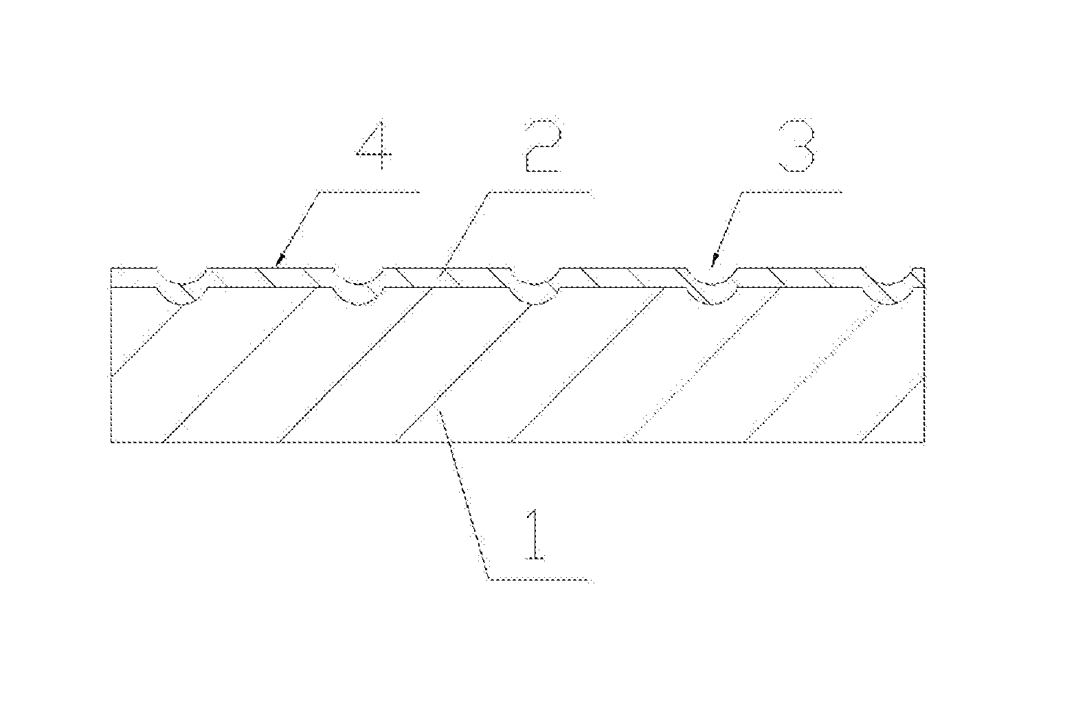
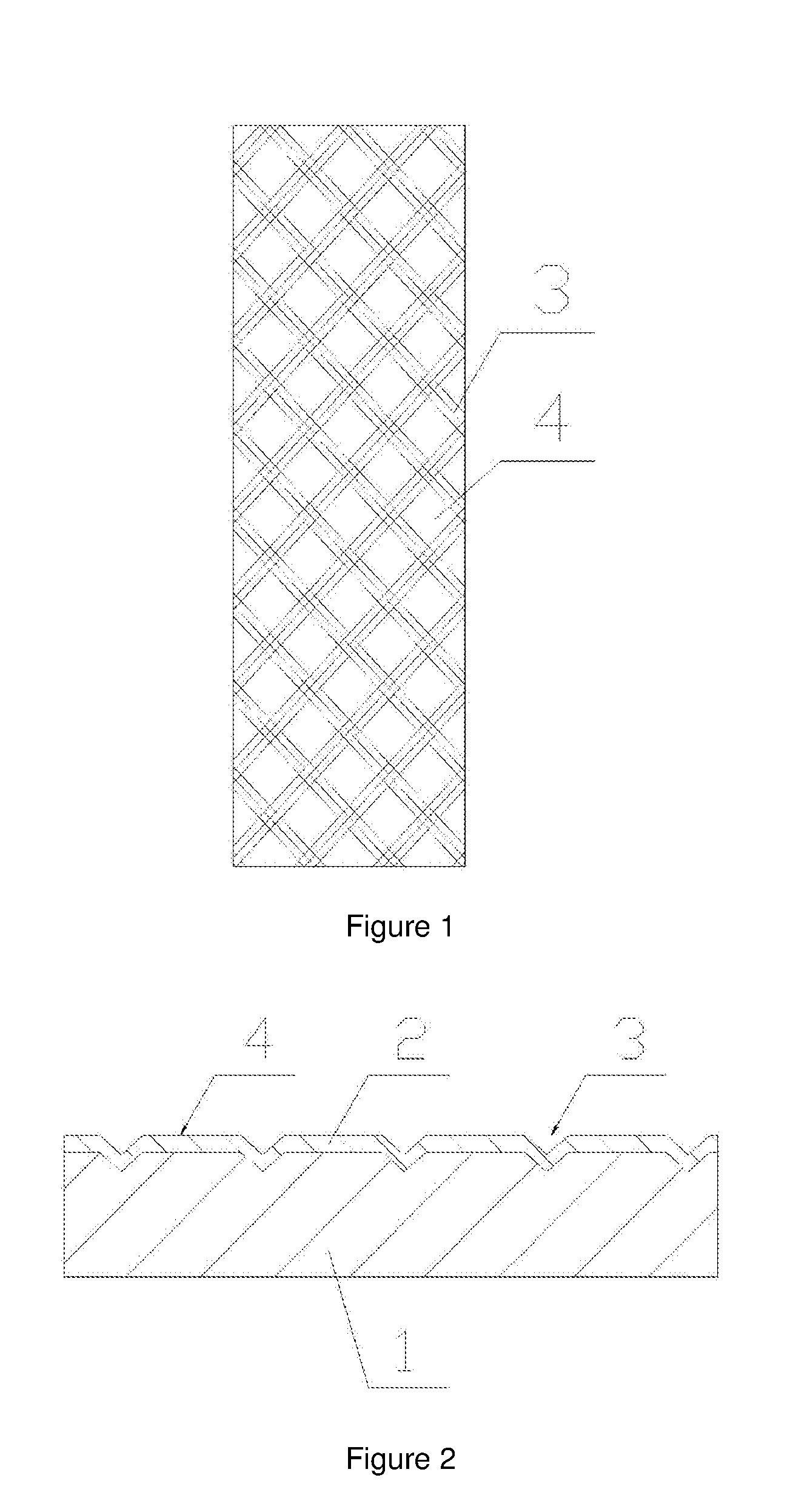
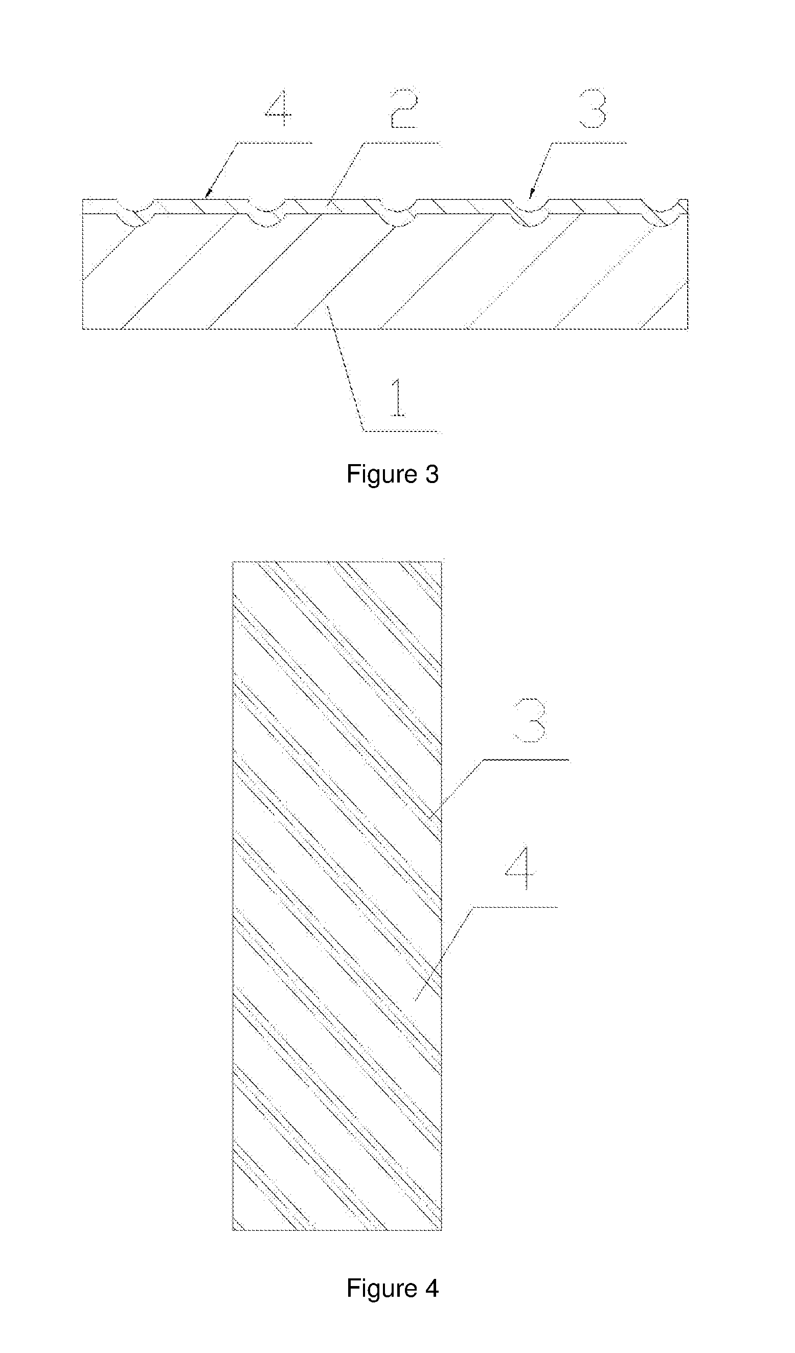
[0035]In this embodiment, TU1 oxygen-free copper is selected to form a conductive base strip with a thickness of 0.22 mm. Linear strip-shaped v-grooves 3 uniformly arranged as intersecting each other are pressed on one or two widthwise surfaces of the conductive base strip. A diamond-shaped flat base strip region 4 is formed between two adjacent grooves 3. A total area of the flat base strip regions 4 on one widthwise surface occupies 35% of a total area of the one widthwise surface of the conductive base strip 1. Each of the linear strip-shaped v-grooves 3 is inclined to both a length direction and a width direction of the conductive base strip 1, and the linear strip-shaped v-grooves 3 are inclined along only two different inclination directions. In the embodiment, linear strip-shaped v-grooves along the two inclination angles mirror each other with respect to the length direction of the conductive base strip 1, and the two inclination angles are substantially 60 degrees to the wi...

embodiment 2

[0045]This embodiment is substantially the same as Embodiment 1, except that the total area of the flat base strip regions 4 on one widthwise surface takes up 30% of the total area of the one widthwise surface of the conductive base strip 1. The grooves 3 are pressed on only one widthwise surface of the conductive base strip, and the depth of each groove 3 is substantially 5% of the thickness of the conductive base strip 1. Moreover, there is an inclination angle of substantially 15 degrees between an inclination direction of linear strip-shaped v-grooves inclined along the two directions and the width direction of the conductive base strip 1.

[0046]When 60 pieces of 156*156 polycrystalline silicon wafer are used to form a group of photovoltaic modules by using the interconnect wire of the invention, a power of such photovoltaic modules is 2.3 W higher than that formed by using a conventional interconnect wire. That is, the power is increased by 1%.

[0047]According to the method for m...

embodiment 3

[0050]This embodiment is substantially the same as Embodiment 1, except that the total area of the flat base strip regions 4 on one widthwise surface takes 70% of the total area of the one widthwise surface of the conductive base strip 1. The grooves 3 are pressed on both the widthwise surfaces of the conductive base strip 1, with the depth of the grooves 3 on one widthwise surface being 20% of the thickness of the conductive base strip 1, and the depth of the grooves 3 on the other widthwise surface being 30% of the thickness of the conductive base strip 1. Moreover, there is an inclination angle of substantially 75 degrees between an inclination direction of linear strip-shaped v-grooves inclined along the two directions and the width direction of the conductive base strip 1.

[0051]When 60 pieces of 156*156 polycrystalline silicon wafer are used to form a group of photovoltaic modules by using the interconnect wire of the invention, a power of such photovoltaic modules is 1.2 W hig...


PUM

PropertyMeasurementUnit
inclination angleaaaaaaaaaa

Abstract

A photovoltaic interconnect wire includes a conductive base strip with grooves provided thereon, and the grooves are linear and/or curved strip-shaped grooves (3) arranged obliquely to a longitudinal direction of the conductive base strip. An inclination angle of 15° to 75° is present between each linear strip-shaped groove and the longitudinal direction of the conductive base strip, and between a tangent line of any point on the curve of a curved-shaped groove and the longitudinal direction of the conductive base strip. The photovoltaic soldering strip increases an output power of a solar cell assembly by increasing the total reflection proportion. It also ensures soldering fastness by adjusting flat regions of the base strip. Effective cross section loss of the conductive base strip is reduced by adjusting the angle of each groove, so as to minimize the confluence efficiency loss of the soldering strip.

Description

TECHNICAL FIELD[0001]The invention relates to the field of photovoltaic interconnect wire fabrication technologies, and particularly to a photovoltaic interconnect wire.BACKGROUND ART[0002]With the rapid development of world economy, energy consumption is ever increasing, and countries in the world are in need of new energy to use widely. The greenhouse effect resulted from carbon dioxide emissions has caused global warming and natural disasters, making demand on clean and renewable energy by countries worldwide very strong. After the global crisis caused by the US subprime mortgage crisis in 2007 became more serious and widespread, each country has taken active measures to encourage the use of renewable energy, so as to stimulate economic growth. The Obama government bid to invest $150 billion into the development of clean energy in the next 10 years. The European Union has set a target that in 2020 renewable energy shall take up to 20% of the total used energy. Japan has proposed ...

Claims


Application Information

Patent Timeline
Patent Type & Authority Applications(United States)
IPC IPC(8): H01L31/05H01L31/054
CPCH01L31/054H01L31/05B23K35/0255B23K35/00H01L31/188Y02E10/52
Inventor QIAN, HAIPENGYU, HAO
Owner FUNDANT JIANGSU ADVANCED MATERIALS CO LTD
Why Eureka
Try Eureka