Optical interconnect apparatuses and electro-optic modulators for processing systems

Inactive Publication Date: 2007-12-06
FUJITSU LTD
View PDF26 Cites 16 Cited by
  • Summary
  • Abstract
  • Description
  • Claims
  • Application Information

AI Technical Summary

Benefits of technology

[0003]Accordingly, there is a need for improved, lower-cost optical interconnect solutions capable of high-speed operation for processing systems and the like.
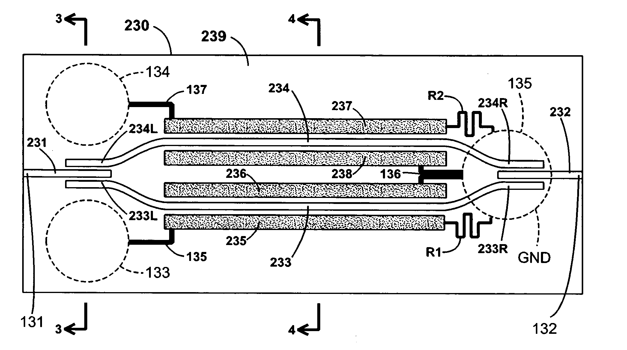
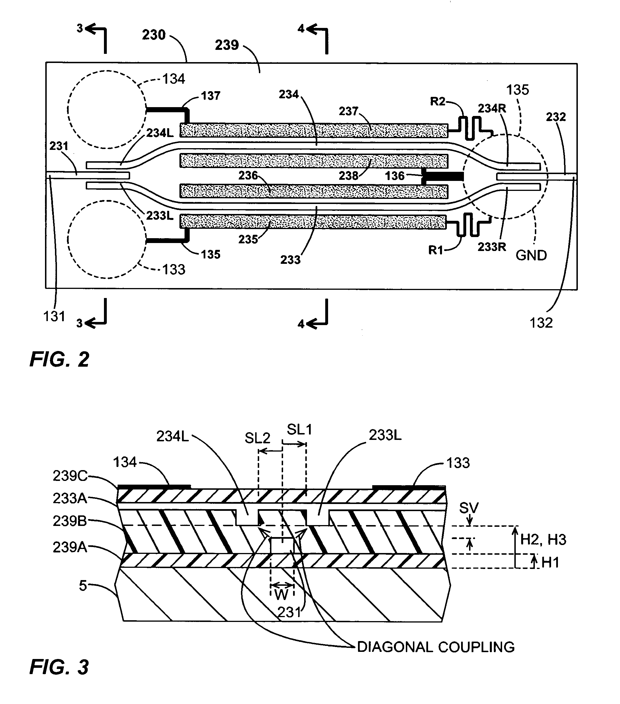
[0004]A first set of inventions of the present application provides a low-loss construction of a Mach-Zehnder Interferometer modulator and similar modulators by configuring an input waveguide core and two branch waveguide cores at different heights above a common substrate so that light is coupled from the input waveguide core to the branch waveguide cores along diagonal directions. The construction enables the input waveguide core to be formed at a different processing layer than the branch waveguide cores, thereby enabling the input waveguide core to be formed with low-loss optical material and the branch waveguides to be formed with an electro-optic material, which can have higher losses than the material of the input waveguide core. Further preferred embodiments may include electrodes disposed near the input waveguide core and the end portions of the branch waveguide cores to enable the degree of coupling to each branch to be adjusted electrically.
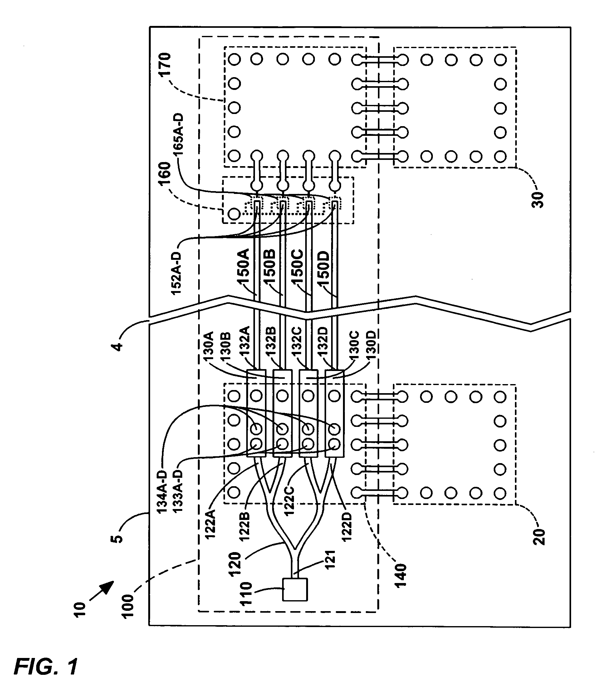
[0005]Another set of inventions of the present application relates to optical interconnect apparatuses for use in a processing system, where the processing system comprises a substrate, a first integrated circuit chip, a second integrated circuit chip, and a need to convey data from the first integrated circuit chip to the second integrated circuit chip. An exemplary optical interconnect apparatus in this set of inventions comprises a semiconductor laser disposed on the substrate and outputting an unmodulated light beam, a waveguide divider having an input optically coupled to said laser and a plurality of outputs, each output providing a respective unmodulated light beam, and a plurality of optical modulators. Each optical mo

Problems solved by technology

Conventional electronic circuits have difficulties in achieving data speeds between components greater than about 10-15 Gbps over any appreciable distance.
While optical systems

Method used


Image

  • Optical interconnect apparatuses and electro-optic modulators for processing systems
  • Optical interconnect apparatuses and electro-optic modulators for processing systems
  • Optical interconnect apparatuses and electro-optic modulators for processing systems

Examples


Embodiment Construction

[0020]In the following description, numerous specific details are set forth to provide a more thorough description of the specific embodiments of the inventions. It is apparent, however, that the inventions may be practiced without all the specific details given below. In other instances, well known features have not been described in detail so as not to obscure the invention.

[0021]Exemplary Interconnect Apparatus 100. A first exemplary embodiment of an optical interconnect apparatus of the present application is shown at 100 in FIG. 1, as illustrated in the context of a processing system 10. System 10 is built on a substrate 5 that houses a plurality of electronic integrated circuit chips whose signals are interconnected to provide a desired system functionality. For the purposes of illustration and without loss of generality, two of the electronic chips are shown at 20 and 30, which are disposed at opposite ends of substrate 5, on opposite sides of a graphical break line 4. In ord...


PUM


Abstract

Disclosed are optical modulators that provide high-speed modulation capability and compact size. In exemplary modulator embodiments, the branch waveguide cores are formed in different processing layers than the input waveguide core, and light is coupled from an input waveguide core to two branch waveguide cores along diagonal directions. The construction enables the input waveguide core to be made of low-loss material compared to the electro-optic material of the branch waveguide cores. Also disclosed are interconnect apparatuses that can be used in processing systems. Exemplary interconnect apparatuses provide various configurations of components that enable high-speed modulation and compact size. The exemplary interconnect apparatuses may use the exemplary optical modulators disclosed herein.

Description

FIELD OF THE INVENTION[0001]The present invention relates to optical interconnect apparatuses for processing systems, such systems including computers, electronic systems boards, opto-electronic systems boards and the like.BACKGROUND OF THE INVENTION[0002]As computers and communication devices become ever faster and the demand for signal communication within processing systems increases, there is a corresponding need to increase the speed of interconnections between the components used in such systems. Conventional electronic circuits have difficulties in achieving data speeds between components greater than about 10-15 Gbps over any appreciable distance. While optical systems can achieve much higher speeds than electronic circuits, they are more expensive to fabricate, and this greater expense has been an obstacle to the use of optical interconnects.SUMMARY OF THE INVENTION[0003]Accordingly, there is a need for improved, lower-cost optical interconnect solutions capable of high-spe...

Claims


Application Information

Patent Timeline
IPC IPC(8): G02F1/035
CPCG02F2001/212G02F1/0356G02F1/212
Inventor GLEBOV, ALEXEILEE, MICHAEL G.ZHOU, DASHUN STEVE
Owner FUJITSU LTD
Why Eureka
Try Eureka