Resistor random access memory cell with reduced active area and reduced contact areas

a memory cell and resistor technology, applied in the direction of basic electric elements, electrical equipment, semiconductor devices, etc., can solve the problems of manufacturing such devices with very small dimensions, and achieve the effects of improving the thermal isolation of the bridge, high thermal conductivity, and increasing the current density of the bridg

Active Publication Date: 2007-12-06
MACRONIX INT CO LTD
View PDF99 Cites 45 Cited by
  • Summary
  • Abstract
  • Description
  • Claims
  • Application Information

AI Technical Summary

Benefits of technology

[0012]The active volume of memory material subject of programmable resistance can be very small. For the purpose of this disclosure, when referring to the dimensions of the structures in the cell, the “length” refers to the distance in the x-direction (left to right in FIG. 1), which for the sidewall insulating member and the sidewall electrodes, is determined by the thicknesses of the spacer layers used to form the sidewalls. The “thickness” of a structure in the cell refers to distance in the y-direction (up and down in FIG. 1), and the “width” refers to distance in the z-direction (perpendicular to the plane of the drawing in FIG. 1). Thus the active volume of memory material is determined by the length of the sidewall insulating member (x-direction), the thickness of the thin film used to form the bridge (y-direction), the width of the bridge orthogonal to the conductive path length (z-direction), and the length of the side wall electrode structures (x-direction) acting as contacts to the bridge. The small contact areas, defined by the lengths of the first and second electrodes and the width of the bridge, improve thermal isolation of the bridge by reducing the area of contact to the electrode material which has relatively high thermal conductivity. The small contact areas also serve to concentrate current flow, increasing current density in the bridge. The improved thermal isolation and increased current density improve reset operation of the cell, particularly for cells comprising bridges of phase change material.
[0013]The length of the side wall electrode structures and the thickness of the thin film of memory material used to form the bridge are determined in embodiments of the technology by thin film thicknesses which are not limited by the lithographic processes used in manufacturing the memory cell. Optionally, the width of the bridge is also smaller than a minimum feature size F that is specified for a lithographic process used in patterning the layer of material in embodiments of the present invention. In one embodiment, the width of the bridge is defined using photoresist trimming technologies in which a mask pattern is used to define a lithographical photoresist structure on the chip having the minimum feature size F, and the photoresist structure is trimmed by isotropic etching to achieve a feature size less than F. The trimmed photoresist structure is then used to lithographically transfer the more narrow pattern onto the layer of insulating material on memory material. Also, other techniques can be used to form narrow lines of material in a layer on an integrated circuit. Accordingly, a phase change memory cell with simple structure achieves very small reset current and low power consumption, and is easily manufactured.

Problems solved by technology

Problems have arisen in manufacturing such devices with very small dimensions, and with variations in process that meet tight specifications needed for large-scale memory devices.

Method used


Image

  • Resistor random access memory cell with reduced active area and reduced contact areas
  • Resistor random access memory cell with reduced active area and reduced contact areas
  • Resistor random access memory cell with reduced active area and reduced contact areas

Examples


Embodiment Construction

[0023]A detailed description of thin film fuse phase change memory cells, arrays of such memory cells, and methods for manufacturing such memory cells, is provided with reference to FIGS. 1-19.

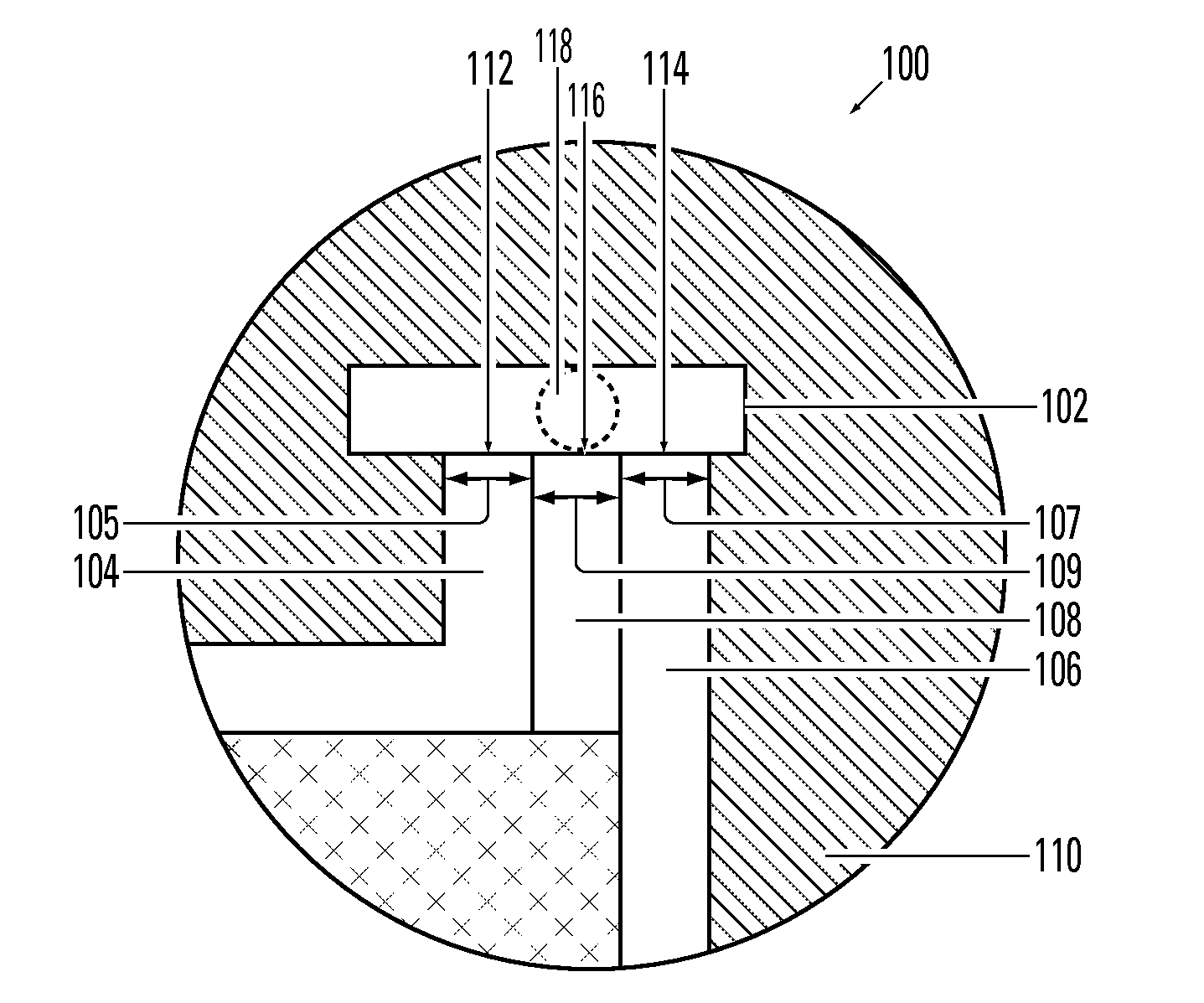
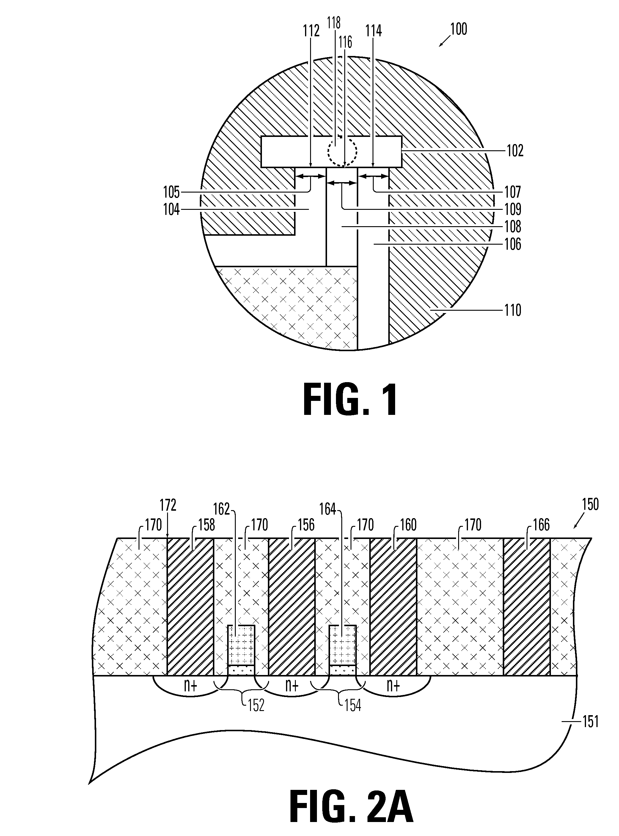
[0024]FIG. 1 illustrates a basic structure of a memory device 100 including a bridge 102 of memory material, such as programmable resistive material on sidewalls of an electrode layer (see FIG. 10, ref. num. 200), which comprises a first electrode 104 having a first electrode length, represented by a double-ended arrow 105, a second electrode 106 having a second electrode length, represented by a double-ended arrow 107, and a sidewall insulating member 108 between the first electrode 104 and the second electrode 106 having a sidewall insulating member length, represented by a double arrow 109. The first electrode length is typically, but not necessarily, essentially the same as the second electrode length, both of which are determined by the thickness of the electrode layer. Similarly, the len...


PUM


Abstract

A memory device has a sidewall insulating member with a sidewall insulating member length according to a first spacer layer thickness. A first electrode formed from a second spacer layer having a first electrode length according to a thickness of a second spacer layer and a second electrode formed from the second spacer layer having a second electrode length according to the thickness of the second spacer layer are formed on sidewalls of the sidewall insulating member. A bridge of memory material having a bridge width extends from a top surface of the first electrode to a top surface of the second electrode across a top surface of the sidewall insulating member, wherein the bridge comprises memory material.

Description

CROSS-REFERENCE TO RELATED APPLICATIONS[0001]This application is related to our co-pending U.S. application Ser. No. ______ filed on the same day as the present application and owned by the same assignee (MXIC 1698-1).BACKGROUND OF THE INVENTION[0002]1. Field of the Invention[0003]The present invention relates to high density memory devices based on phase change based memory materials, including chalcogenide based materials and on other programmable resistive materials, and to methods for manufacturing such devices.[0004]2. Description of Related Art[0005]Phase change based memory materials are widely used in read-write optical disks. These materials have at least two solid phases, including for example a generally amorphous solid phase and a generally crystalline solid phase. Laser pulses are used in read-write optical disks to switch between phases and to read the optical properties of the material after the phase change.[0006]Phase change based memory materials, like chalcogenide...

Claims


Application Information

Patent Timeline
Patent Type & Authority Applications(United States)
IPC IPC(8): H01L21/8242
CPCH01L45/04H01L45/06H01L45/1226H01L45/14H01L45/144Y10S438/90H01L45/147H01L45/1625H01L45/1675H01L27/2436H01L45/146H10B63/30H10N70/231H10N70/20H10N70/823H10N70/881H10N70/8828H10N70/8833H10N70/8836H10N70/026H10N70/063
Inventor LAI, ERH-KUNHO, CHIAHUAHSIEH, KUANG YEU
Owner MACRONIX INT CO LTD
Why Eureka
Try Eureka