
Liquid crystal display element

a liquid crystal display and display element technology, applied in liquid crystal compositions, instruments, chemistry apparatuses and processes, etc., can solve the problems of increasing scattering of light, reducing transmittance, and difficult to achieve full focal conic state, so as to reduce electric power consumption, reduce driving voltage, and expand the operating temperature range

Active Publication Date: 2007-12-13
IRIS OPTRONICS INC
View PDF5 Cites 14 Cited by
  • Summary
  • Abstract
  • Description
  • Claims
  • Application Information

AI Technical Summary

Benefits of technology

[0028] As described above, there are problems to be solved in order to achieve, lowered driving voltage, expanded operating temperature range, reduced electric power consumption and wide range of display maintaining temperature of a liquid crystal display element.
[0033] By this aspect of the present invention, it is possible to obtain a liquid crystal display element using a cholesteric liquid crystal having features such as semi-permanent display maintaining function (memory function), bright color display, high contrast and high resolution, wherein one or more of lowered driving voltage, expanded operating temperature range, reduced electric power consumption and wide range of display maintaining temperature are achieved.

Problems solved by technology

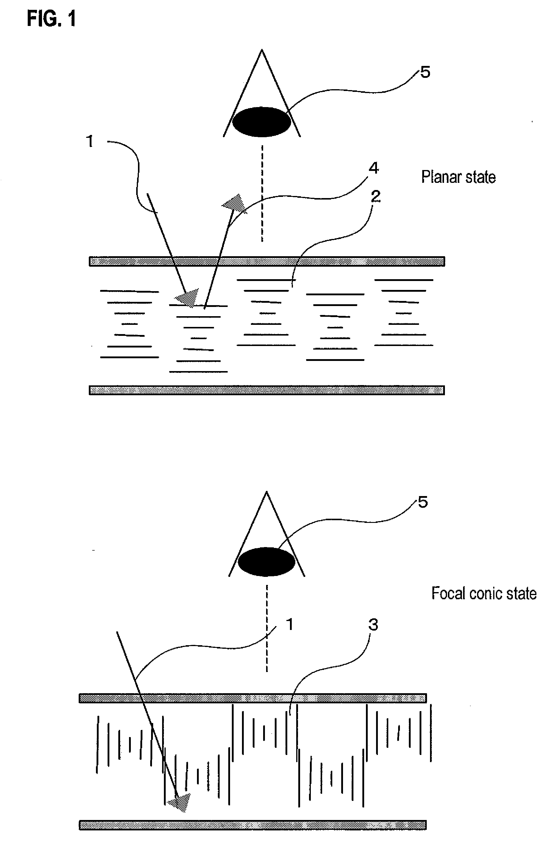
When the viscosity becomes even higher, a full focal conic state becomes hard to achieve, decreasing the transmittance and increasing scattering of light.
Due to such circumstances, desired contrast is not provided sometimes when a liquid crystal display element is driven at a low temperature.
Liquid crystal display elements using cholesteric liquid crystals have some problems in practice as follows.
On this account, costs for parts for the driving circuit are rather high.

Method used


Image

  • Liquid crystal display element
  • Liquid crystal display element
  • Liquid crystal display element

Examples


example 1

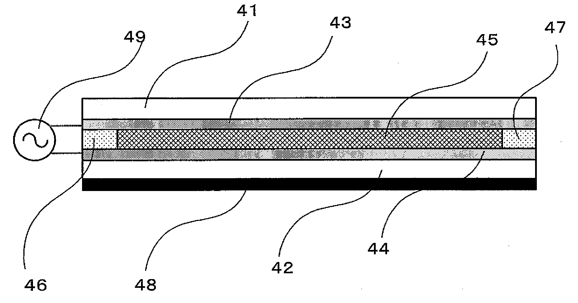
[0101] Patterning in a stripe shape at a 0.24 mm pitch was made by etching on two ITO transparent electrodes installed on polycarbonate (PC) film substrates having a cut size of 12×10 cm so that VGA display with 640×480 dots could be shown. The area formed by the overlapping of these pair of electrodes when seen from the direction perpendicular to the display screen of the liquid crystal display element was 135 cm2.

[0102] Afterwards, a polyimide alignment control film material was applied onto the transparent electrodes of both substrates to a thickness of about 700 angstrom (converted value being about 70 nm) by spin coating. Then, baking treatment was carried out in a oven at 90° C. for one hour to form the alignment control films. The electrostatic capacity of each alignment control film was then calculated to be about 2.5 μF, and the sum was about 5 μF. This alignment control film had a volume resistance value of about 1016 Ω·CM. It is considered to be an insulating thin film a...

example 2

[0113] A liquid crystal display element using a 3 μm-diameter spacer that had a size of about 2×1 cm was prepared (other conditions being the same as EXAMPLE 1) as a display part for IC cards. The result is shown in FIG. 6. The abscissa axis in FIG. 6 represents the temperature at the time of driving, and the ordinate axis represents the driving voltage. The driving voltages on or above the line which connects data represented by ▴ marks refer to driving voltages that can realize a complete planar state, the driving voltages between the line connecting the data represented by ▪ marks and the line connecting the data represented by ♦ marks refer to driving voltages that can realize a complete focal conic state.

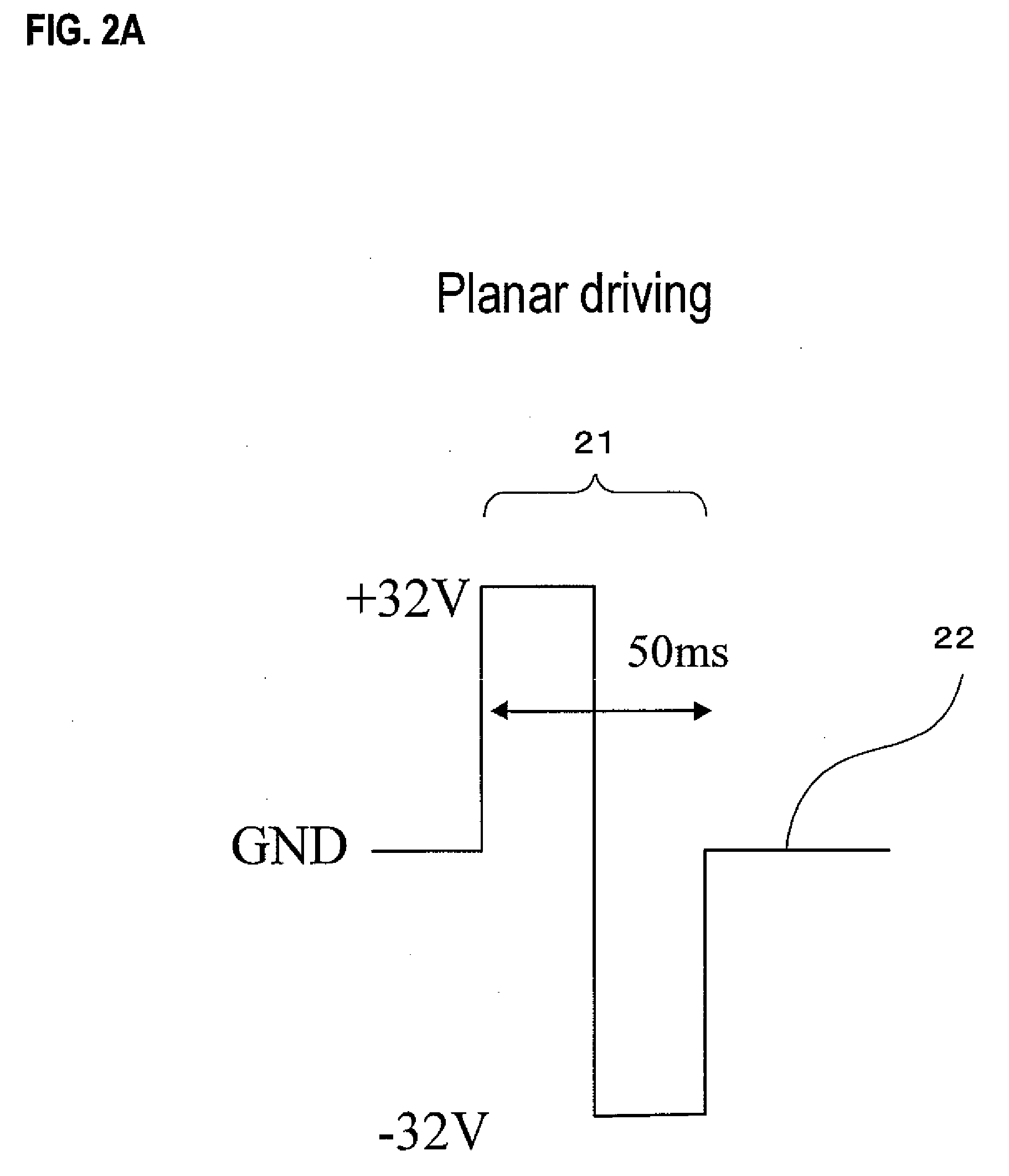
[0114] It is understood from FIG. 6 that in such a liquid crystal display element, when a pulse voltage having a driving voltage of 14 V and an effective time of 50 milliseconds, for example, was applied at temperatures in the range of 0 to 50° C., the selected state (planar s...

example 3

[0118] In the following experiments, liquid crystal display elements were prepared as in EXAMPLE 1, except that the compositions of liquid crystals and chiral agents were changed variously.

[0119]FIG. 7 is a graph showing the relationship between the Δ∈ / viscosity of the liquid crystal composition according to the present invention and the driving voltage. It is understood that the condition of a driving voltage not more than 32V is satisfied by Δ∈≧20 and the viscosity≦1200 mPa·s as in the present invention.

[0120]FIG. 8 is a graph showing the relationship between the viscosity and contrast. It shows a case in which when the viscosity >1200 mPa·s at a low temperature, the transmittance of the focal conic state falls (that is, scattering is increased), and the contrast decreases sharply.

[0121] In addition to this, when the specific resistance of the liquid crystal was less than 1010, the electric power consumption at the time of driving increased greatly, and the wireless driving bec...


PUM

PropertyMeasurementUnit
thicknessaaaaaaaaaa
isotropic phase transition temperatureaaaaaaaaaa

Abstract

A liquid crystal display element according to the present invention includes one or more sets of combinations of a pair of substrates, a liquid crystal layer composed of a liquid crystal composition indicating a cholesteric phase and disposed between the pair of substrates, and at least one layer of insulating thin film to insulate the liquid crystal layer from an electrode, wherein: the insulating thin film has an electrostatic capacity of not more than 10 μF; the liquid crystal layer has a layer thickness in the range of 2 to 5 μm; and the liquid crystal composition has a dielectric anisotropy in the range of 20 to 50. The present invention can realize at least one of lowered driving voltage, enlarged operating temperature range, decrease in electric power consumption and wide display maintaining temperature range, in a liquid crystal display element having a semi-permanent display maintaining function (memory function).

Description

CROSS-REFERENCE TO RELATED APPLICATIONS [0001] This application is a continuation of International Application No. PCT / JP2005 / 002690, filed on Feb. 21, 2005, now pending, herein incorporated by reference.BACKGROUND OF THE INVENTION [0002] 1. Field of the Invention [0003] The present invention relates to a liquid crystal display element using a cholesteric liquid crystal. [0004] 2. Description of the Related Art [0005] Recently, the development of electronic paper has been advancing vigorously in business organizations and universities. For the electronic paper application markets that are expected, proposed are various application forms including electronic books heading the list, sub-displays for mobile terminals, display parts for IC cards, etc. [0006] One of the most promising modes for the electronic paper is one using a cholesteric liquid crystal. Cholesteric liquid crystals have excellent characteristics such as semi-permanent display maintaining function (memory function), br...

Claims


Application Information

Patent Timeline
Patent Type & Authority Applications(United States)
IPC IPC(8): C09K19/02G02F1/1333
CPCG02F1/133345G02F1/13718G02F1/1347
Inventor NOSE, MASAKITOMITA, JUNJI
Owner IRIS OPTRONICS INC
Learn More