
Fabrication process for crystalline zinc oxide semiconductor layer

a technology of crystalline zinc oxide and fabrication process, which is applied in the direction of semiconductor devices, electrical equipment, basic electric elements, etc., can solve the problems of high equipment investment, complex processing techniques, and high cost of conventional fabrication processes for crystalline zinc oxide semiconductor layers

Inactive Publication Date: 2007-12-13
XEROX CORP
View PDF0 Cites 168 Cited by
  • Summary
  • Abstract
  • Description
  • Claims
  • Application Information

AI Technical Summary

Benefits of technology

[0020]wherein the at least one semiconductor layer is formed by a semiconductor fabrication process comprising: liquid depositing one or more zinc oxide-precursor compositions and forming the at least one semiconductor layer of the thin film transistor comprising crystalline zinc oxide preferentially oriented with the c-axis perpendicular to the plane of the at least one semiconductor layer from the liquid deposited one or more zinc oxide-precursor compositions.

Problems solved by technology

But to produce high-mobility TFTs, conventional fabrication processes for a zinc oxide semiconductor layer for TFTs may be costly, involving high equipment investment and complex processing techniques.

Method used


Image

  • Fabrication process for crystalline zinc oxide semiconductor layer
  • Fabrication process for crystalline zinc oxide semiconductor layer
  • Fabrication process for crystalline zinc oxide semiconductor layer

Examples


example 1

[0076]A 0.05M-0.2 M solution of zinc acetate in a mixture of ethanolamine and methoxyethanol (with Zn / amine=1 molar ratio) was first prepared by adding methoxyethanol to a mixture of zinc acetate dihydrate dihydrate (1.10 g, 5 mmol) and ethanolamine (0.32 g, 5 mmol), followed by heating at 60° C. for 1 hr to dissolve the solid.

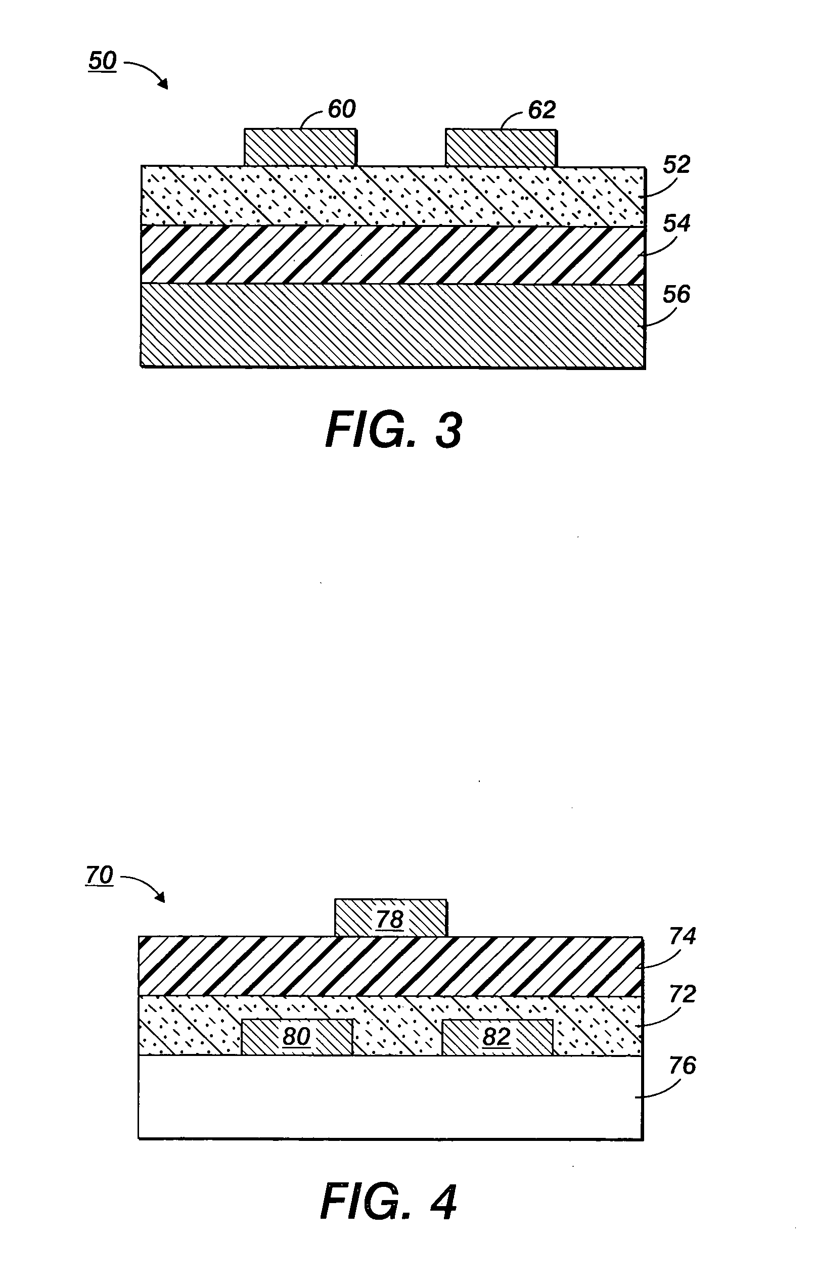
[0077]A TFT device having the configuration of FIG. 3 was prepared as follows. A glass substrate coated with an indium-tin oxide (ITO) layer and an aluminum-tin oxide (ATO, 100 nm) top layer was first cleaned with oxygen plasma and then drop-coated with a 0.05 M zinc acetate solution, spun on a spin-coater at a speed of 1000 rpm for 2 minutes, and then heated on a hot plate at 180° C. for 30 min. It was then placed in a pre-heated oven at 400° C. for 30 min. The coating and heating procedures were repeated twice using respectively 0.1 M and 0.2 M zinc acetate solutions. Finally, an array of aluminum source-drain electrode pairs with channel length of 90 micron...


PUM

PropertyMeasurementUnit
temperatureaaaaaaaaaa
deformation temperatureaaaaaaaaaa

Abstract

A process for fabricating at least one semiconductor layer of a thin film transistor composed of: liquid depositing one or more zinc oxide-precursor compositions and forming the at least one semiconductor layer of the thin film transistor including crystalline zinc oxide preferentially oriented with the c-axis perpendicular to the plane of the at least one semiconductor layer from the liquid deposited one or more zinc oxide-precursor compositions.

Description

BACKGROUND OF THE INVENTION[0001]Zinc oxide is a promising channel semiconductor in thin film transistors (“TFTs”) for fabricating low cost TFT circuits for large area displays and other low cost electronics. But to produce high-mobility TFTs, conventional fabrication processes for a zinc oxide semiconductor layer for TFTs may be costly, involving high equipment investment and complex processing techniques. Thus, there is a need addressed by embodiments of the present invention for simpler, less costly fabrication processes for a zinc oxide semiconductor layer which can result in TFTs with high field-effect mobility.[0002]The following documents provide background information:[0003]E. Fortunato et al., “Fully Transparent ZnO Thin-Film Transistor Produced at Room Temperature,”Adv. Mater., Vol. 17, No. 5, pp. 590-594 (Mar. 8, 2005).[0004]T. E. Park et al., “Structural and Optical Properties of ZnO Thin Films Grown by RF Magnetron Sputtering on Si Substrates,”J. Korean Phys. Soc., Vol....

Claims


Application Information

Patent Timeline
Patent Type & Authority Applications(United States)
IPC IPC(8): H01L21/16H01L21/00
CPCH01L21/02554H01L29/7869H01L21/02628H01L29/045
Inventor ONG, BENG S.LI, YUNINGWU, YILIANG
Owner XEROX CORP
Features
  • Generate Ideas
  • Intellectual Property
  • Life Sciences
  • Materials
  • Tech Scout
  • Unparalleled Data Quality
  • Higher Quality Content
  • 60% Fewer Hallucinations
Learn More